SOPHIA ANTIPOLIS, France – December 18, 2023 │ The GaN newsletter for December 2023 is now available! This monthly newsletter allows you to keep up to date on the latest scientific publications, patent applications, and news related to III-Nitride semiconductors (GaN, AlN, InN, and alloys) for optoelectronic and electronic applications (power, RF, LED, laser, photonics, and so on). This month, let us highlight Intel’s latest developments in GaN electronics to address the increasing power density and efficiency needs of data centers and networking platforms.
Intel advances GaN IC technology for power management
In December’s issue, KnowMade reports on a recent news from Intel. At IEDM 2023, the company introduced its DR (driver) GaN or DrGaN, which monolithically integrates a CMOS driver with GaN power switches on a 300mm GaN-on-Si platform. This work shows that it is possible to co-integrate the Si PMOS transistor with GaN transistors while maintaining the high figure of merit (FoM) to keep up with the growth of power density. According to the company, the new DrGaN device can address the power requirements of future CPUs and GPUs, showing excellent resistance and leakage performance. This is made possible by the development of a new gate-last process flow for 3D monolithic integration of GaN and Si CMOS, that leverages layer transfer technology (Figure 1). Interestingly, using this technological approach, Intel circumvents the challenging task of fabricating p-channel GaN devices, that would be required in a DrGaN device integrally made of GaN.
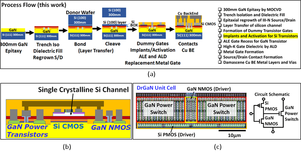
Figure 1: (a) The new process flow for the 3D monolithic integration of GaN and Si CMOS by layer transfer. (b) The new 3D monolithic integration of GaN and Si CMOS by this process. (c) The layout of a 40×10µm2 180nm DrGaN unit cell. Source: Paper 9.7, “DrGaN: an Integrated CMOS Driver-GaN Power Switch Technology on 300mm GaN-on-Si with E-mode GaN MOSHEMT and 3D Monolithic Si PMOS,” H.W. Then et al, Intel, IEDM 2023.
Yet this approach also rises major challenges related to the integration of Si and GaN technologies, especially challenges due to the thermal budget of their respective processes. As shown in Figure 1, Intel aims to address this challenge by completing the high-temperature activation steps for the Si CMOS transistors before depositing the GaN transistor’s gate dielectric. What’s more, this method allows GaN and Si CMOS transistors to share the same backend interconnect stack, which reduces resistance and mask count. With a FoM of 0.59 (mΩ-nC)-1 for a 30nm gate-length GaN MOS-HEMT, the new technology exhibits a promising potential for future scaling of the architecture.
This achievement is another milestone after previous breakthroughs in RF and power GaN technologies. It accelerated in 2018/2019 with the first report on the development of a 300-mm GaN-on-Si technology, dedicated to power supply of user equipment and future use of mmW frequencies for wireless LAN capability. Last year, Intel announced a 20X improvement over state-of-the-art e-mode p-GaN HEMT in a key FoM for power delivery (Figure 2). Concomitantly, with the same device architecture, Intel announced record cutoff frequencies, a critical FoM for communications.
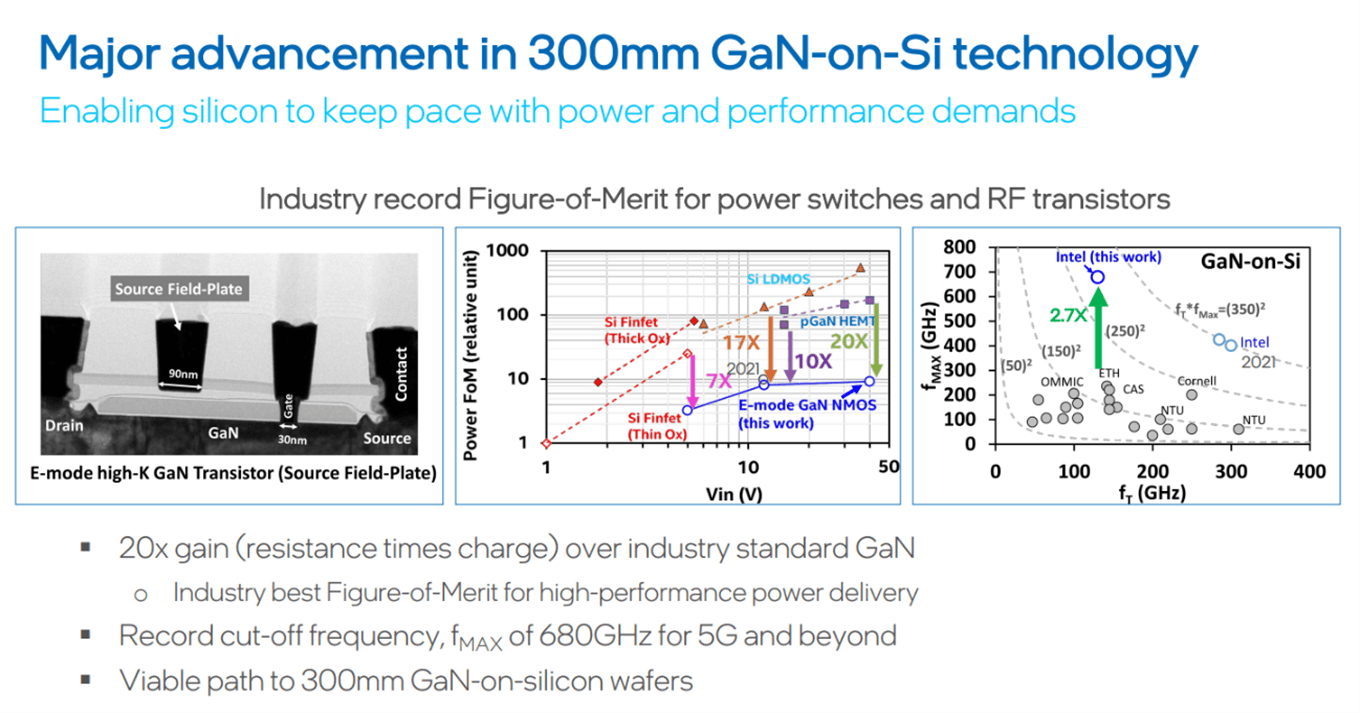
Figure 2: Intel’s previous research breakthroughs introduced at IEDM 2022. Source: Scaled submicron field-plated e-mode high-K GaN transistors on 300mm Si(111) wafer with power FoM (RON xQGG) of 3.1 mohm-nC at 40V and fT/fMAX of 130/680GHz, IEEE Int. Electron Devices Meeting Tech. Dig., 111 (2022), pp. 35.1.1-35.1.4.
In the power GaN landscape, Intel competes with Navitas, Cambridge GaN Devices (CGD), EPC and others that have been developing power GaN integrated circuits (IC). Yet Intel stands out as the only company to focus on harnessing efficiency of GaN for 48V and below, according to Paul Fisher, Director of Chip Mesoscale Process Development at the Components Research at Intel. In the RF GaN landscape, Intel stands out as one of the main players actively pushing GaN-on-Si technology with Infineon, MACOM, GlobalFoundries and others. Their advances in GaN devices and circuits at higher mm-wave frequencies were reviewed by a recent paper from Fraunhofer IAF and Albert-Ludwigs-Universität Freiburg that KnowMade reported in the GaN newsletter earlier this year. What’s more, apart from the recent conference papers, Intel published a couple of scientific papers in 2023, describing e-mode 300-mm GaN-on-Si(111) with integrated Si CMOS, for future mm-wave RF applications (published in April) and dealing with the assessment of T-Gate and Π -Gate HEMT, through cellular Monte Carlo simulations (co-published with Arizona State University in September). In the first paper, Intel’s principal engineer Han Wui Then et al. reported a new record fMAX = 700 GHz ( fT = 115 GHz) with an LG = 50 nm GaN MOS-HEMT having a submicrometric source field plate fabricated using a 300-mm GaN MOS-HEMT process with integrated Si CMOS.
Intel has resumed its IP activities in GaN electronics
KnowMade recently published a GaN electronics IP report analyzing both RF and power GaN patent landscapes. Intel entered the GaN electronics patent landscape in 2013 and accelerated its IP strategy in 2017-2019 (Figure 3), with a focus on GaN-on-Si technology. While GaN-on-Si is the mainstream platform for power applications, it has not been adopted yet in RF applications, where the GaN-on-SiC platform dominates. KnowMade’s report analyzed the position of the main players in the RF GaN IP competition. Interestingly, Intel stands as one of the best-established players for GaN-on-Si epiwafers, and as an undisputable leader for GaN-on-Si devices, far ahead of its main challengers such as MACOM and TSMC.
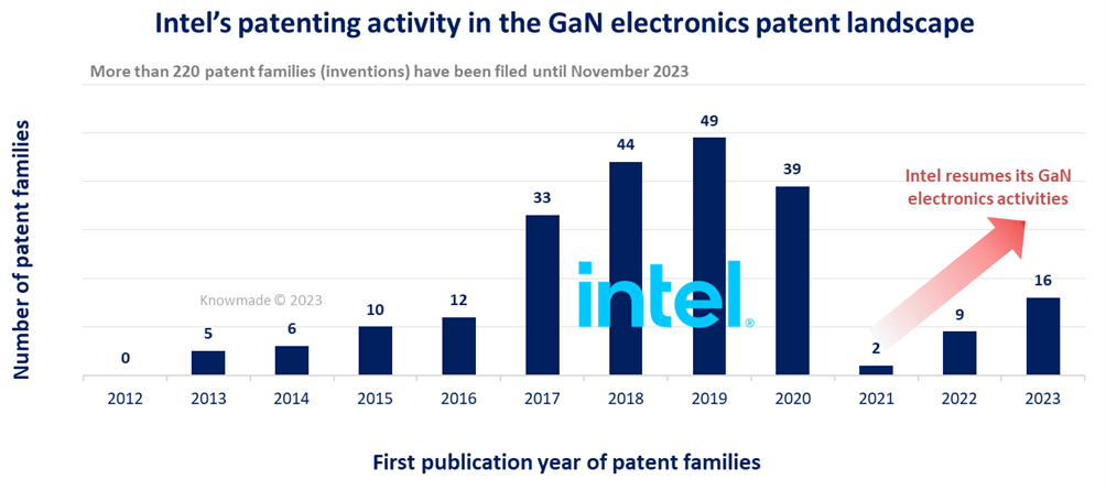
Figure 3: Intel’s patenting activity in the GaN electronics patent landscape (source: GaN electronics patent landscape report, KnowMade, November2023)
The number of GaN electronics patent publications abruptly dropped in 2021, following COVID-19 pandemic. This sharp decrease in patent filings has not been observed only for GaN electronics, since Intel’s patent filings overall dropped by 50% from 2019 to 2020. Yet Intel has maintained most of its GaN electronics patents alive during this break. What’s more, Intel has resumed its patenting activity in the GaN electronics field lately, confirming the position of GaN electronics in its technology roadmap. Indeed, more than 15 new patent applications were published by Intel in 2023, identified in KnowMade’s GaN newsletter and analyzed in more details in KnowMade’s GaN electronics patent monitor. This inventive activity is led by two main inventors: Principal Engineer Han Wui Then and Integration Group Leader Marko Radosavljevic. The recent patent publications describe several inventions leveraging layer transfer technology for GaN IC fabrication, such as US20230090106, US20230069054, US20230197732 and US20230054719. Furthermore, other recent inventions address critical aspects of the gate structure (e.g., patent US20230197840, Figure 4).
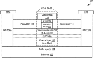
Figure 4: Gate structure to enable lower subthreshold slope in GaN transistors (US20230197840)
Eventually, the GaN electronics IP report highlights an IP strategy centered on the US (200+ patent applications) and Taiwan (90+). Intel’s patenting activity for GaN electronics has been relatively limited in other countries. Yet the strongest progression in patent filings is presently seen in Europe, which is consistent with the recent ambitions of Intel to expand its activities in Europe, from R&D and manufacturing all the way to packaging.
Press contact
contact@knowmade.fr
Le Drakkar, 2405 route des Dolines, 06560 Valbonne Sophia Antipolis, France
www.knowmade.com
About the author
Rémi Comyn works for KnowMade as a Patent Analyst in the field of Compound Semiconductors and Electronics. He holds a PhD in Physics from the University of Nice Sophia Antipolis (France) in partnership with CRHEA-CNRS (Sophia Antipolis, France) and the University of Sherbrooke (Québec, Canada). Rémi previously worked in compound semiconductors research laboratory as Research Engineer.
About KnowMade
KnowMade is a Technology Intelligence and IP Strategy consulting company specialized in analysis of patents and scientific information. The company helps innovative companies and R&D organizations to understand their competitive landscape, follow technology trends, and find out opportunities and threats in terms of technology and patents.
KnowMade’s analysts combine their strong technology expertise and in-depth knowledge of patents with powerful analytics tools and methodologies to turn patents and scientific information into business-oriented report for decision makers working in R&D, Innovation Strategy, Intellectual Property, and Marketing. Our experts provide prior art search, patent landscape analysis, scientific literature analysis, patent valuation, IP due diligence and freedom-to-operate analysis. In parallel the company proposes litigation/licensing support, technology scouting and IP/technology watch service.
KnowMade has a solid expertise in Compound Semiconductors, Power Electronics, Batteries, RF Technologies & Wireless Communications, Solid-State Lighting & Display, Photonics, Memories, MEMS & Solid-State Sensors/Actuators, Semiconductor Manufacturing, Packaging & Assembly, Medical Devices, Medical Imaging, Microfluidics, Biotechnology, Pharmaceutics, and Agri-Food.