KnowMade provides various resources related to Gallium Nitride (GaN) technologies, which is a rapidly developing field:
- Get free insights into GaN industry from a patent perspective.
- Explore the emerging ecosystems for GaN technology through our comprehensive reports.
- Stay updated on the latest R&D and IP developments in the field taking advantages of our monitoring services.
Insights

SOPHIA ANTIPOLIS, France – June 10, 2025 │ KnowMade today announced the publication of its Q1 2025 IP report on GaN electronics, highlighting robust patenting activity [...]
SOPHIA ANTIPOLIS, France – July 30, 2024 │ GaN electronic devices, especially GaN-based high electron mobility transistors (HEMT), are increasingly used in RF and power [...]

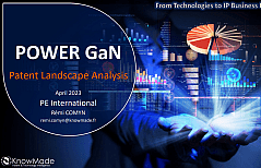
SOPHIA ANTIPOLIS, France – April 25, 2024 │Get an update on the Power GaN patent landscape with Dr. Rémi Comyn. He gave an online lecture, [...]
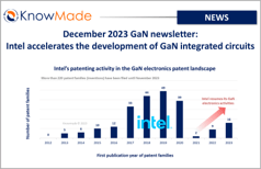
SOPHIA ANTIPOLIS, France – December 18, 2023 │ The GaN newsletter for December 2023 is now available! This monthly newsletter allows you to keep up [...]
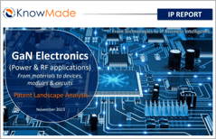
SOPHIA ANTIPOLIS, France – December 5, 2023 │ Knowmade is releasing a new GaN intellectual property (IP) report providing a deep dive into the power [...]
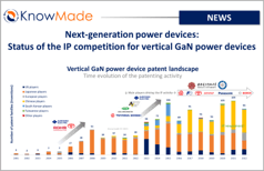
SOPHIA ANTIPOLIS, France – November 29, 2023 │ Gallium nitride (GaN) power devices were successfully adopted in several power applications, starting with lateral GaN devices. [...]
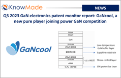
SOPHIA ANTIPOLIS, France – November 16, 2023 │ The quarterly report for Q3 2023 GaN Electronics patent monitor is now available. This monitoring service allows [...]
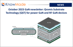
SOPHIA ANTIPOLIS, France – October 27, 2023 │The GaN newsletter for October 2023 is now available! This monthly newsletter allows you to keep up to [...]
Reports
 |
 |
| GaN Electronics Patent Lansdcape Analysis | Next-Generation Power Modules Patent Landscape 2021 |
Monitors
 |
 |
| GaN Electronics Patent Monitoring Service | GaN Newsletter |
Conferences
 |
| PE International 2023: our analyst’s intervention |
Book contribution
 |
| GaN Technology |