SOPHIA ANTIPOLIS, France – November 16, 2023 │ The quarterly report for Q3 2023 GaN Electronics patent monitor is now available. This monitoring service allows you to keep up to date on GaN-related patent activity for RF & Power electronics: new patent publications, newly granted patents, patents expired or abandoned, latest patent transfers and patent litigation.
This quarter, let us focus on a new entrant in the power GaN IP landscape: GaNcool.
Anticipating opportunities and risks through patent watch
Gallium nitride (GaN) is the technology of choice for applications that require high frequency, high voltage, and high-power density. GaN has made impressive progress in material and process technologies, resulting in significant improvements in device performance for both power and RF applications. Today, more and more companies are adopting GaN devices into their electronics components, making GaN market more competitive. Patenting your innovative technology grants you a monopoly on your invention and protect it from its use by competitors in countries where your patent is in force. However, you also must be sure that what you intend to put on the market is not in the claims’ scope of patents from competitors. To manage that risk, Knowmade provides you with a reliable GaN Electronics patent monitoring service, which regularly follows patents from publication, and granting until they expire or are abandoned. Our quarterly patent monitor’s reports and databases not only give you a clear vision of your competitors’ strategies and future intentions, but also help you keep track of the latest technology and early detect new entrants in your business field. Through our GaN Electronics patent monitor, you can visualize existing technology and its trends that inform your present strategy and help you build a business strategy suitable for the future market.
Power GaN applications drive the GaN electronics patent activities
In our quarterly analysis, the GaN electronics patents are categorized into different segments of applications, supply chains, and technical challenges. The temporal evolution of new patent applications by segments reflects the level of investment in R&D and helps you visualize the technological and market trends. Let’s take an example of application segmentation, in which the new patent families (inventions) are divided into RF and power applications.
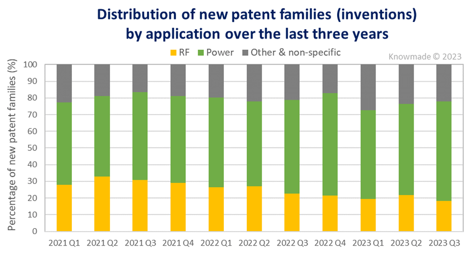
Figure 1: Distribution of new patent families by application over the last three years (source: Knowmade’s GaN Electronics Quarterly Patent Monitor).
It is obviously seen in figure 1 that, over the last three years, from 2021 to 2023, the share of new patent publications related to GaN RF fell slowly from 30% to 20% of the total published GaN electronics patents whereas the space of GaN power tended to increase from 50% to 60%. To meet the growing demands for automotive, e-mobility, and power supply for data centers, GaN intellectual property (IP) leaders such as Mitsubishi Electric, Texas Instruments, Infineon, Rohm, Innoscience, and Fuji Electric, have stepped up their patent activities in power GaN applications since 2021. Additionally, new entrants, mainly from China, are also focusing on expanding their IP activities for power GaN applications. In Q3 2023, over 15 IP newcomers were identified in GaN electronics patent landscape, more than half of them are Chinese entities, with around 60% of their new inventions related to power applications. Among the IP newcomers, we noticed a GaN pure player – GaNcool – whose patent publications are analyzed in the following section.
GaNcool, a new GaN pure player entering power GaN competition
GaNcool (Fuzhou Gallium Valley Semiconductor, 福州镓谷半导体, www.gancool.com) was founded in 2022 by former Bell Labs scientists and Chinese semiconductor experts according to its corporate website. In Q3 2023, GaNcool published its first five domestic patent applications. The names of the inventors, Zhu Qing (祝庆) and Feng Wenjun (冯文军), do not provide additional information about the background of GaNcool’s founders mentioned above. Yet in a press release from Fuzhou New Area earlier this year, Hu Liang (梁琥), is introduced as the current CTO of GaNcool. Hu Liang, who graduated from Hong Kong University of Science and Technology and Beijing Normal University, is also director of the epitaxy department of another GaN company in Europe, BelGaN. What’s more, he previously worked at imec for which he filed two GaN electronics patent applications (US10636882, US10312083). The inventions deal with III-nitride selective growth methods using masking layers, which can be used for the fabrication of GaN transistors. As such, they belong to the same field as the inventions disclosed by GaNcool this quarter.
GaNcool focuses on the development and production of GaN wafers intended to produce integrated circuits. It claims to have reached the status of mass production for GaN-on-Si wafers, and to have on-going developments for GaN-on-sapphire and GaN-on-SiC platforms. When GaN is grown on foreign substrates, the mismatches in lattice constants and thermal expansion coefficients lead to high defect density, deformation, wrapping or even cracks. This prevents the use of these substrates in high power applications. To overcome this bottleneck, GaNcool provides a method of using double-sided growth technology on sapphire substrates. As claimed in the patent application CN116544194 published in Q3 2023, the GaN epitaxial layer is grown on the front side of the substrate, and stress control layer followed by a SiN protective layer are prefabricated on the back side of the substrates (Figure 2). The stress control layer includes a low-temperature GaN buffer layer, a 3D GaN layer and an undoped GaN layer, in which the thickness of the undoped GaN layer is tuned to compensate for the tensile stress created by the GaN epitaxial layer. According to the inventors, the wrapping degree is significantly reduced, providing crack-free epilayers for the fabrication of high-power devices.
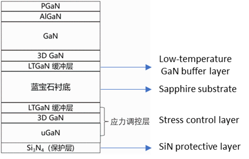
Figure 2: Schematic diagram of double-sided growth technology of GaN-on-sapphire adapted from GaNcool’s patent application CN116544194.
Although the lateral GaN-on-Si devices have gained a great space in power applications, their markets are still limited to the low voltage range (650 V and under). Vertical GaN devices are proposed to overcome the voltage limitations of the lateral devices. To expand its IP strategy to high voltage applications, GaNcool has developed some methods for the fabrication of vertical GaN devices, with four new patent publications identified in Q3 2023. These inventions provide technical solutions to overcome i) poor activation of the p-GaN layer (CN116705607), ii) surface damage at the bottom and the side wall of the gate trench caused by etching (CN116544105), iii) early breakdown due to current crowding (CN116741810), iv) GaN etching or decomposition during cooling down and the introduction of impurities to the GaN surface during device processing (CN116825619).
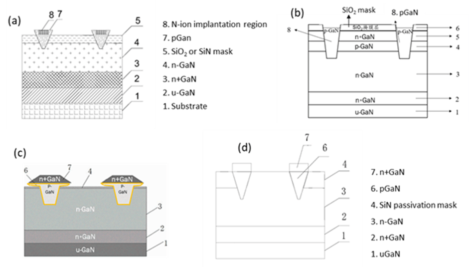
Figure 3: (a), (b), (c), (d) Schematic diagrams of the vertical GaN structures adapted from GaNcool patent applications CN116705607, CN116544105, CN116741810, CN116825619, respectively.
In the conventional vertical GaN device, high p-doped GaN is still difficult to achieve due to poor activation of the p-GaN layer. In the patent application CN116705607, GaNcool uses a SiO2 or SiN mask to form a deposition groove on the n-GaN top layer (Figure 3 (a)). Then a trapezoid-shaped p-GaN layer is grown into the deposition groove with a height higher than the mask layer. After N-ions are implanted into the surface of the p-GaN layer, the ions are activated through an annealing process. It is well known that the Mg-doped p-GaN grown by MOCVD is usually activated by annealing the sample with gases to break the strong Mg-H bonding and activate the Mg acceptor. In conventional structures, the p-GaN layer is generally covered by epitaxial layers (cap layers, for example), that prevent the action of the annealing to break the Mg-H bonding. In this invention, the trapezoid-shaped increases the surface contact area of the p-GaN layer with the annealing gases, thereby promoting the activation process.
For vertical GaN power transistors, the gate trench is generally formed by plasma etching which introduces additional surface damage at the bottom and side walls of the groove. That will cause an increase in interface defects, abnormal electrical performance, and problems with the instability and reliability of the gate. To solve the damage caused by dry etching, GaNcool’s inventors developed an etching process using synchronous growth in the MOCVD (CN116544105). In this invention, after patterning the SiO2 to reveal the GaN surface, the wafer is transferred into the MOCVD, where it is exposed to the H2, NH3, and trimethyl gallium (TMG) gases. The gas flows of H2 and TMG are controlled to have GaN etching and growth at the same time, in which the etching rate is greater than the growth rate. This method provides a gate trench with minimized surface damage. Then a p-GaN layer can be grown into the groove, as shown in Figure 3 (b). Using this technique, after etching, the wafer is not taken out of the MOCVD, and groove surface treatment is directly carried out in the MOCVD. So, besides providing a groove with a smooth surface, the method also prevents the introduction of impurities and additional oxidation of the interface, caused by the exposure of the wafer to the air.
Using the etching process claimed in the patent application CN116544105, GaNcool then develops a method to grow an p-GaN/n+-GaN heterostructure into the groove with a larger interface (CN116741810). In this invention, after the groove is formed by the etching process in the MOCVD reactor, a p-GaN layer is grown on the periphery of the groove with a mushroom head structure. Then, a n+ GaN layer with a trapezoid shape is grown on top of the p-GaN layer (Figure 3(c)). This method can increase the interface between p-GaN and n+-GaN layers, leading to an increase in current spreading and limiting the occurrence of current breakdown in GaN electronic devices based on this structure.
Furthermore, GaNcool disclosed the growth of an in-situ SiN passivation mask on top of a vertical GaN structure (CN116825619). Different from the three other inventions where the SiO2 or SiN masks are deposited by using PECVD, in this invention the SiN passivation mask is formed directly on top of the n-GaN layer after the heterostructure is grown in the MOCVD reactor (Figure 3 (d)). The advantage pertained to this invention is that the GaN surface is protected by the SiN mask from any etching or decomposition when the temperature is reduced. The SiN mask also prevents the introduction of impurities on the GaN surface during the device processing. Additionally, the SiN mask and the GaN layer have good matching performance, so the problems of cracking caused by differences in thermal expansion can also be avoided.
A patent monitoring service to help you track competitors’ IP activity and detect weak signals
The GaN Electronics Patent Monitor provides up-to-date data on patent activity for RF & Power electronics. This monitoring service allows you to take advantage of a quarterly-updated Excel database and benefit from both quarterly analysis reports and direct access to our analysts for on-demand discussions regarding the results, trends, specific patented technologies, or companies’ patent portfolios in the field of GaN electronics.
The GaN Electronics Quarterly Patent Monitor can be subscribed to at any time directly from here. If you need more information, reach us at contact@knowmade.fr or with our contact forms.
Press contact
contact@knowmade.fr
Le Drakkar, 2405 route des Dolines, 06560 Sophia Antipolis, France
www.knowmade.com
About the author
Huong NGO, PhD., works at KnowMade as a Patent Analyst in the field of Compound Semiconductors and Optoelectronics. She holds a PhD in Physics from the University of Montpellier (France). Huong previously worked at Meijo University (Japan), CRHEA-CNRS (France), and Lafayette Institute (France) as Research Engineer.
About KnowMade
KnowMade is a Technology Intelligence and IP Strategy consulting company specialized in analyzing patents and scientific publications. The company helps innovative companies, investors, and R&D organizations to understand their competitive landscape, follow technological evolutions, reduce uncertainties, and identify opportunities and risks in terms of technology and intellectual property.
KnowMade’s analysts combine their strong technology expertise and in-depth knowledge of patents with powerful analytics tools and methodologies to turn patent information and scientific literature into actionable insights, providing high added value reports for decision makers working in R&D, innovation strategy, intellectual property, and marketing. Our experts provide prior art search, patent landscape analysis, freedom-to-operate analysis, IP due diligence, and monitoring services.
KnowMade has a solid expertise in Compound Semiconductors, Power Electronics, Batteries, RF Technologies & Wireless Communications, Solid-State Lighting & Display, Photonics, Memories, MEMS & Sensors, Semiconductor Packaging, Medical Devices, Medical Imaging, Microfluidics, Biotechnology, Pharmaceutics, and Agri-Food.