SOPHIA ANTIPOLIS, France – October 27, 2023 │The GaN newsletter for October 2023 is now available! This monthly newsletter allows you to keep up to date on the latest scientific publications, patent applications, and news related to III-Nitride semiconductors (GaN, AlN, InN, and alloys) for optoelectronic and electronic applications (power, RF, LED, laser, photonics, and so on).
This month, let us highlight the latest developments related to QST substrate technology for power GaN and RF GaN devices.
Qromis’ QST engineered substrate for GaN power electronics.
During heteroepitaxy, the lattice-constant and thermal-expansion-coefficient (CTE) mismatch between the epitaxial layer and the substrate results in the generation of defects either during growth or during cooling from growth temperature to room temperature. Qromis Substrate Technology (QST) solves the limitations of CTE mismatch by employing a core wafer CTE and presenting a Si (111) surface for GaN epitaxy. The CTE-matched core is made of poly-AlN ceramic and is surrounded by several dielectric layers (Thermal Management of Gallium Nitride Electronics, Woodhead Publishing P. 251-274). Following that, another dielectric layer is produced to create a smooth surface on which a (111)-oriented Si layer is bonded. This Si surface is epi-ready, which allows the application of well-developed GaN-on-Si technology to grow thick GaN layers, which is essential for the manufacture of high-performance GaN power electronics.
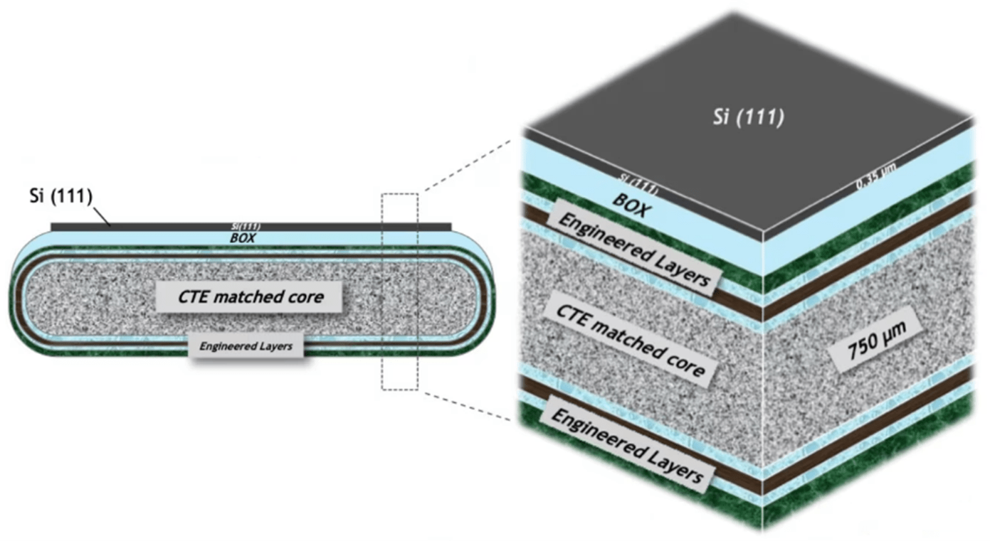
Figure 1: The structure of QST engineered substrate (source: Qromis)
IMEC and Aixtron report 8.5 µm-thick GaN layers on 200 mm QST substrate.
In the latest scientific publication section of our GaN newsletter, we noticed that IMEC and AIXTRON research teams have successfully grown 5 µm GaN drift layers on 200-mm QST wafers in an AIXTRON G5+ C Planetary Reactor (5 x200 mm standard configuration). Optimized growth conditions result in GaN epitaxial layers that have low defect density and great uniformity, with total thicknesses of up to 8.5 µm. Using this structure, a semi-vertical diode with a breakdown voltage of 750 V is achieved. The growth of a high-quality thick GaN layer on the QST substrate enables higher breakdown voltages and better thermal management, making it a promising solution for vertical power devices.
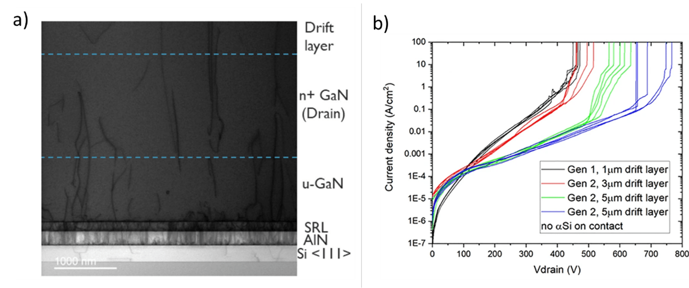
Figure 2: (a) Cross-sectional SEM of GaN epitaxial layers grown on a QST substrate and (b) Back-to-back diodes reverse leakage and breakdown. (source: W Gonçalez Filho et. al., Sci Rep 13, 15931 (2023))
Shin-Etsu’s QST platform for power GaN and RF GaN markets
One of the notable press releases in this month’s GaN newsletter is that Shin-Etsu, a worldwide chemical company, announced its market entry strategy for GaN power devices. Besides the sales of QST substrates, Shin-Etsu Chemical will also provide GaN-on-QST wafers with diameters of 6 inches and 8 inches (wafers of 12-inch diameter are in development). In addition, the company also developed a technology that enables the growth of a 20 μm-thick GaN layer and facilitates the achievement of power devices with a breakdown voltage of 1800 V. Furthermore, Shin-Etsu Chemical cooperated with Oki Electric and succeeded in developing a method that allows the exfoliation of a thick layer of high-quality GaN from an insulating QST substrate and bonding it to other substrates. This method paves the way for the fabrication of high-power, high-quality vertical devices on 200-mm substrates. This will promote the manufacture of power devices with high yields and competitive pricing.
To support its market strategy, Shin-Etsu took a license on QST technology from Qromis while filing several patents related to this innovative technology. Although Shin-Etsu’s recent press release focuses on the power GaN market, its recent patenting activity indicates that the company also started advancing the QST platform for RF applications, anticipating new opportunities in the emerging RF GaN market. In this month’s GaN newsletter, we report Shin-Etsu’s new patent application WO2023/176185 which aims to improve the thermal conductivity and the mechanical strength of QST substrates. For that purpose, the inventors make possible the bonding of a modified type of AlN ceramic core (including fiber-like AlN single crystal) to a Si<111> seed layer via a flat sealing layer and a planarization layer. As a result, the thermal conductivity can be increased from 170 W/mK (upper limit of polycrystalline AlN ceramics) to 200 W/mK for AlN ceramics in which monocrystalline AlN fibers are introduced. Likewise, the fracture toughness of the AlN ceramic core can be improved from 3 MPa.m1/2 to 10 Mpa.m.1/2. What’s more the warping issue is alleviated, which may translate into a higher yield and lower cost for such epiwafers. These improvements promote the GaN-on-QST platform in demanding applications such as automotive applications and RF applications where thermal management remains critical. Especially, this new QST platform can be optimized to reduce high-frequency losses, by introducing a high-resistivity Si<111> seed layer (> 1 kΩ.cm), as claimed by Shin Etsu’s inventors in this new patent application.
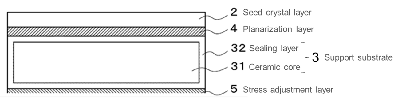
Figure 3: Adapted drawing from Shin-Etsu’s patent application WO2023/176185
Vanguard International Semiconductor QST related patent activity
Another company, Vanguard International Semiconductor (VIS), a Taiwanese leader in IC foundry, also got the license from Qromis for QST technology in 2018. In previous months, VIS published a new patent application related to GaN-on-QST for power applications (US20230170389). The invention aims to prevent the Si seed layer from generating a back gating effect in the GaN HEMT and is applicable to GaN-on-QST or GaN-on-SOI platforms. In the October 2023 GaN newsletter, we report a new patent application from VIS related to QST substrates (US20230299146). The invention describes a superlattice buffer structure that prevents warpage and stabilizes the curvature of GaN epiwafers based on Si, SOI and QST substrates, on a wide range of thicknesses. According to VIS’ inventors, this structure is particularly suitable for high-power RF GaN-HEMTs, where a superlattice layer with thinner thickness and small bow variation is usually required to improve RF characteristics.
A GaN newsletter to help you make your way in various dynamic competitive landscapes
With the monthly GaN newsletter, KnowMade provides a cost-efficient way to access the different players’ recent R&D activities and latest collaborations, to have a complete picture of their strategies to enter the market at the right time, with the right products, and to detect new players worldwide early on. Combining both patent and paper analyses provides answers to many questions you might have about the players in your ecosystem. In the end, the GaN newsletter is also about detecting timely new threats and opportunities for your activities. As such, the GaN newsletter is valuable for researchers, engineers, and IP professionals, but it is also a powerful tool in the hands of marketing and innovation strategists and commercial teams.
The GaN newsletter can be subscribed to at any time directly from here. For more information about the GaN newsletter, please contact us at contact@knowmade.fr.
Press contact
contact@knowmade.fr
Le Drakkar, 2405 route des Dolines, 06560 Sophia Antipolis, France
www.knowmade.com
About the author
Rémi Comyn, PhD., works at KnowMade as a Patent Analyst in the field of Compound Semiconductors and Electronics. He holds a PhD in Physics from the University of Nice Sophia-Antipolis (France) in partnership with CRHEA-CNRS (Sophia-Antipolis, France) and the University of Sherbrooke (Québec, Canada). Rémi previously worked in compound semiconductors research laboratory as Research Engineer.
Huong NGO, PhD., works at KnowMade as a Patent Analyst in the field of Compound Semiconductors and Optoelectronics. She holds a PhD in Physics from the University of Montpellier (France). Huong previously worked at Meijo University (Japan), CRHEA-CNRS (France), and Lafayette Institute (France) as Research Engineer.
About KnowMade
KnowMade is a Technology Intelligence and IP Strategy consulting company specialized in analyzing patents and scientific publications. The company helps innovative companies, investors, and R&D organizations to understand their competitive landscape, follow technological evolutions, reduce uncertainties, and identify opportunities and risks in terms of technology and intellectual property.
KnowMade’s analysts combine their strong technology expertise and in-depth knowledge of patents with powerful analytics tools and methodologies to turn patent information and scientific literature into actionable insights, providing high added value reports for decision makers working in R&D, innovation strategy, intellectual property, and marketing. Our experts provide prior art search, patent landscape analysis, freedom-to-operate analysis, IP due diligence, and monitoring services.
KnowMade has a solid expertise in Compound Semiconductors, Power Electronics, Batteries, RF Technologies & Wireless Communications, Solid-State Lighting & Display, Photonics, Memories, MEMS & Sensors, Semiconductor Packaging, Medical Devices, Medical Imaging, Microfluidics, Biotechnology, Pharmaceutics, and Agri-Food.