August 25, 2022

KnowMade’s expertise in memory technology

Bit demand will continue to grow, promising new technologies are appearing, and new applications open new opportunities

Memory technology is a key enabler to support the digital transformation driven by global megatrends such as the internet of things (IoT) for connected, smart or wearable electronics, artificial intelligence (AI) / machine learning (ML), and data centers. The demand for memory chips, while decreasing in the short term due to the current over-supply on the memory market, will continue to grow in the mid-to-long term, as investments are going on to meet the requirements of the AI/ML, big data and metaverse industries.

Challenges for memory technology

Higher data storage density (scaling), bandwidth capability (speed), power management (energy consumption) and cost are critical factors that drive current memory technology developments. There are currently two main approaches to address these challenges: advanced packaging and memory engineering.

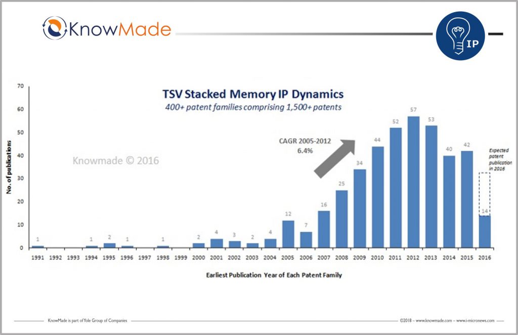
In standard data handling architectures, data is transferred between processing units and memory.  This causes performance loss in terms of speed and energy, and these issues worsen with the data quantity required for new applications (big data, AI/ML, etc.). To address the so-called “memory bottleneck”, new solutions aim to bring the data processing unit and memory unit closer to one another. In advanced packaging, innovative integration of memory and processing units greatly improve the chip performance and allow ultra-high computing power and ultra-low power consumption. Several competing memory packaging approaches are being explored. High-bandwidth memory (HBM) leverages 3D-stacking of memory dies using through-silicon vias (TSVs). At the same time, the R&D on hybrid bonding is carried out to vertically connect die-to-wafer (D2W) or wafer-to-wafer (W2W) via closely spaced copper pads. Major memory manufacturers have R&D activities on such a wafer-to-wafer stacking approach and significant technical challenges still need to be addressed. Another possibility to improve performance is to process data within the memory device. In this context, emerging non-volatile memories (NVM) are intensively investigated as they can enable “in-memory computing”. Also appreciated for more standard low-power applications, additional challenges lay ahead for these new memory technologies to gain larger market shares. Scaling to smaller nodes is key to achieving higher density memory, thus major semiconductor players regularly disclose inventive ways of manufacturing those devices to secure a smaller footprint. Finally, as emerging NVM are based on new structures and new materials, more work is needed to optimize them and harness the full potential of that promising technology.

KnowMade’s purpose

At KnowMade, we investigate and monitor patents and scientific literature to keep track of the semiconductor memory technology and ecosystem evolutions, with a close eye on new technology developments and applications such as emerging non-volatile memories (NVM), high-performance computing (HPC) and artificial intelligence (AI) / machine learning (ML). Our patent landscape analyses aim to provide the big picture of what is going on in the memory field, and a comprehensive view of what the technological and competitive landscape could look like in the next few years. We can provide a tailored analysis or monitoring service designed according to your needs to dive into specific memory technologies and/or companies, and to follow, on a monthly or quarterly basis, IP and R&D activities all year around. We are able to carry out prior-art searches for either patentability or invalidation projects, technical reviews, identify critical patents, perform freedom-to-operate (FTO) analysis to evaluate the IP risks, and conduct evidence-of-use searches (patent-to-product mapping) for your patent enforcement/licensing campaign.

Our memory device expertise includes static random access memory (SRAM), dynamic random access memory (DRAM, 3D DRAM), flash memory (planar, 3D NAND), emerging NVM, phase change memory (PCRAM or PCM), resistive switching random access memory (RRAM or ReRAM), oxide resistive random access memory (OxRRAM), conductive bridge random access memory (CBRAM), 3D XPoint, memristor, crossbar architecture, magnetoresistive random access memory (MRAM, SOT-MRAM, STT-MRAM), ferroelectric random access memory (FRAM, FeRAM), ferroelectric field-effect transistors (FeFET), 2D materials-based memory, synaptic transistors, selectors (transistor, ovonic threshold switching OTS), etc.


Latest reports on memory

Featured image of Memory for AI patent landscape.
Are there specific memory technologies claimed in patents that are more suitable than others for artificial intelligence/machine learning (AI/ML) applications? Who are the key patent [...]
The 3D Non-Volatile Memory field is changing fast. How the Chinese players can find a place in a crowded space? Publication March 2018 Download Flyer [...]
The semiconductor industry has all the attributes that appeal to patent licensing companies (PLCs): Are you in their sights? Publication February 2017 Download Flyer Download [...]

Patent monitors on various semiconductor technologies

Featured image of GaN newsletter.
Every month, the GaN newsletter provides you with a selection of the latest scientific publications, patent applications and news related to III-Nitride semiconductors (GaN, AlN, [...]
Featured image of RF Front end patent monitor.
Get updated data on RF front-end module patent activity: new patents, patents expired or abandoned, latest patent transfers and patent litigation. Need more information or [...]
Featured image of GaN electronics patent monitor.
Get updated data on GaN-related patent activity for RF & Power electronics: New patent applications, patents newly granted, expired or abandoned patents, latest patent transfers, [...]

Latest insights on memory

Featured image of article: Newcomers protecting memory hardware innovations for Artificial Intelligence: how do their patent portfolio looks like? How do they compare to big firms?
SOPHIA ANTIPOLIS, France – June 06, 2023 │ Since 2015, the number of new inventions for artificial intelligence applications focused on memory hardware has been [...]
Featured image of article Physical Unclonable Functions (PUFs): a short review of innovators who are making the digital revolution more secure.
SOPHIA ANTIPOLIS, France - December 19, 2022 │ The need for a strong security and authentication solution for the connected world creates new opportunities for [...]
SOPHIA ANTIPOLIS, France – January 12, 2017| 3D is becoming a key technology platform for increase integration, either for heterogeneous integration (like for MEMS and [...]

June 6, 2023

Newcomers protecting memory hardware innovations for Artificial Intelligence: how do their patent portfolio looks like? How do they compare to big firms?

SOPHIA ANTIPOLIS, France – June 06, 2023 │ Since 2015, the number of new inventions for artificial intelligence applications focused on memory hardware has been booming. Here we look at the non-volatile memories, which are intensively investigated by semiconductor companies. Numerous patent applications relate to device fabrication, system architecture, selectors, and testing, and address major technical bottlenecks. While fierce competition exists between key semiconductor players like Samsung or IBM, newcomers are sneaking in. In this article, we shed light on the intellectual property (IP) activity of one of the newcomers, TetraMem.

The competitive IP landscape is diversifying

As the floods of data are becoming more and more important, the need for high performance computing has become stringent. Among the cutting-edge technologies driving innovation in the semiconductor industry, neuromorphic computing has emerged as a promising possibility, that could enable data management in a more effective manner. Large integrated device manufacturers (IDMs) and memory makers, like Samsung or IBM, own broad patent portfolio of memory technologies that can be used for artificial intelligence (AI) applications: magnetoresistive random-access memory (MRAM), phase-change memory (PCM), resistive random-access memory (RRAM or memristors), ferroelectric random-access memory (FeRAM), or ferroelectric field-effect transistor (FeFET). In our latest research, not only did we find that established semiconductor IP players are strong leaders in developing memory for AI, but those big companies also keep a heads up in more path finding activity with 2D materials (Samsung) and synaptic transistor (IBM). In addition, with a detailed look at the patent applicants over the last three years, we identified newcomers sneaking in the patent landscape. The competitive IP landscape of memory technologies for AI applications is clearly diversifying: the start-ups TetraMem and ICLeague, the equipment supplier Applied Materials, and even established IC foundries have joined the competition. IP profiles of main semiconductor industrials and newcomers have been reviewed in KnowMade’s report Memory for Artificial Intelligence Patent Landscape Analysis 2023.

Bar chart showing the ranking of companies according to their ownership of patent families.

Figure 1: Ranking of industrial patent assignees according to the number of their patent families (inventions) related to memory technologies for artificial intelligence (AI) applications. Source: KnowMade, Memory for Artificial Intelligence Patent Landscape Analysis 2023.

A closer look at TetraMem, a newcomer joining the innovation competition

While leading IP players are publishing new patent applications on a broad range of emerging memory technologies, newcomers are sneaking in the patent landscape quietly, with a focused technology portfolio. One example sticking out from our detailed IP landscape on memory for AI is TetraMem.

TetraMem is a pure-player start-up company founded in 2018. As the company was set up by Hewlett-Packard (HP) former employees, it beneficiates from a strong RRAM expertise, builds on HP experience, and moves fast towards high-density RRAM integration. The patent portfolio focuses on RRAM device integration in crossbar memory arrays for in-memory computing and selectors associated to the RRAM cells. In a high-density network of RRAM cells integrated in crossbar memory arrays, one of the technical challenges is the presence of large parasitic currents. Sneak path current may trigger unwanted actions (e.g., unintended programming) and may prevent desirable outputs (e.g., read errors). As a result of these technical issues, during a neuromorphic computing process for instance, computation results may be altered. In a detailed analysis of TetraMem patented inventions, KnowMade reveals that the start-up is mainly protecting technologies (RRAM device, selector device, circuit design) that address the sneak path current challenge for improved reliability in crossbar memory arrays and is making fast progress. Additionally, TetraMem is seeking IP protection for reliable and low power RRAM devices. Innovation has accelerated, taking the technological lead is becoming more and more important for semiconductor companies.

Comparison of patents held by Samsung and TetraMem in the field of memory for AI applications.

Figure 2: Comparison of the patent portfolio related to memory technologies for AI applications held by established IP player Samsung vs. IP newcomer TetraMem. Source: KnowMade, Memory for Artificial Intelligence Patent Landscape Analysis 2023.

Memory hardware development targeting artificial intelligence technology deployment is a blooming field of innovation. The ecosystem is diversifying with all kinds of companies from start-ups to established players, to IC semiconductor industrials and equipment suppliers. Lots of companies are intensifying their patenting activity to secure their share of the AI market. Further analysis is required to get the big picture. Who is taking the lead and is there a specific technology more favorable than others for AI application? Unique IP portfolios analysis combined with high technical expertise is giving us a competitive insight on what is happening in the field. Check out KnowMade’s analysis on this topic: Memory for Artificial Intelligence Patent Landscape Analysis 2023.

You may be also interested in:

Are there specific memory technologies claimed in patents that are more suitable than others for artificial intelligence/machine learning (AI/ML) applications?

Physical Unclonable Functions (PUFs): a short review of innovators who are making the digital revolution more secure

Other related memory patent landscape reports


Press contact
contact@knowmade.fr
Le Drakkar, 2405 route des Dolines, 06560 Valbonne Sophia Antipolis, France
www.knowmade.com

About the author
Pauline Calka, PhD. works for KnowMade as a patent analyst in the fields of semiconductor manufacturing and advanced packaging. She holds a PhD in Memory from the University of Grenoble Alpes (France), in partnership with the CEA-Leti (France). After an Alexander von Humboldt Postdoc fellowship position at the Technical University of Berlin (Germany) and the Leibniz Institute for High Performance Microelectronics on ReRAM development, Pauline worked five years at ASM International (Belgium) as Senior Process Engineer on thin film development for logic, memory and MEMS, and two years at CEA-Leti as Integration Engineer on imaging CMOS sensors.

About KnowMade
KnowMade is a technology intelligence and IP strategy consulting company specialized in analyzing patents and scientific publications. The company helps innovative companies, investors, and R&D organizations to understand competitive landscape, follow technological evolutions, reduce uncertainties, and identify opportunities and risks in terms of technology and intellectual property.
KnowMade’s analysts combine their strong technology expertise and in-depth knowledge of patents with powerful analytics tools and methodologies to turn patent information and scientific literature into actionable insights, providing high added value reports for decision makers working in R&D, innovation strategy, intellectual property, and marketing. Our experts provide prior art search, patent landscape analysis, freedom-to-operate analysis, IP due diligence, and monitoring services.
KnowMade has a solid expertise in Compound Semiconductors, Power Electronics, Batteries, RF Technologies & Wireless Communications, Solid-State Lighting & Display, Photonics, Memories, MEMS & Sensors, Semiconductor Packaging, Medical Devices, Medical Imaging, Microfluidics, Biotechnology, Pharmaceutics, and Agri-Food.

December 19, 2022

Physical Unclonable Functions (PUFs): a short review of innovators who are making the digital revolution more secure

SOPHIA ANTIPOLIS, France – December 19, 2022 │ The need for a strong security and authentication solution for the connected world creates new opportunities for both memory and IC players. With different technology offers and new companies coming in, competition is getting fiercer by the day, as we have seen by analyzing the patents in this field.

Introduction to physically unclonable functions

With the rapid rollout of digitization in everyday life, data security is a growing concern. Connected objects are processing and storing lots of information that could be hacked remotely and misused, leading to critical data theft and safety issues.

Nowadays, transportation – both public and private – is optimized with the use of on-board advanced electronics, enabling safer and more comfortable driving. The need for automotive cybersecurity is increasing in parallel to the development of connected cars. Some data security issues must be considered for artificial intelligence applications, with the risk of edge AI devices being manipulated remotely, compromising the AI-driven system. One may think of the consequences for assisted medical devices, smart cities, or big data processed in servers. At the same time, there is also strong demand for greater privacy of personal user information in mobile computing devices (computers, smartphones).

A key enabler for new technology deployment

In this context, there has been growing demand for secure storage. Among the possibilities, semiconductor companies have recently been promoting the use of so-called Physical Unclonable Functions (PUFs). PUFs are hardware structures designed to utilize the random physical variations which occur naturally in a semiconductor device during the manufacturing process. Because of the uncontrollable and unpredictable nature of these random disorders, building a clone of the device is considered impractical. Like a human fingerprint, a PUF can be considered an inherent and unique identifier of every IC chip. When manufactured, the PUF will be fed a series of different challenges and have its responses recorded. Through this exercise, the designers know each PUF’s unique response to a given challenge and can use this information to prevent counterfeiting, and create and store cryptographic keys. Additionally, an attack would be identified since a PUF would have its physical properties affected by the attack.

Bar chart showing the increase in patent applications related to PUFs (physical unclonable functions).

Figure 1: Time evolution of PUF-related patent applications published over the past two decades.

Fierce competition for physical unclonable function memory market share

Recent public communications and intellectual property (IP) developments are pointing to memory-based PUFs as a hot topic in the semiconductor industry. Both standard and emerging memory technologies are engineered for PUF applications. The IP protection business is thriving: PUF technology can be licensed from several companies including eMemory (or its subsidiary PUFsecurity), Intrinsic ID and others. We present here a short overview of the available PUF hardware and related patents.

PUFs based on standard memory technologies

While numerous technologies can operate as PUF keys, the most common hardware approach available today is to exploit the randomness of characteristics of semiconductor static random-access memory (SRAM).

The behavior of an SRAM cell depends on the difference in the threshold voltages of its transistors. Intrinsic ID, founded in 2008 as a spinout from Philips Research, is a leading provider of PUF focused on SRAM storage technology. Its SRAM PUFs use unique identity transistor threshold voltage as an identifier thanks to deep submicron variation that occurs naturally during manufacturing. Intrinsic ID has acquired several critical patents filed by Philips from 2003-2008, and today the company owns almost 30 granted patents that enable invention protection in the US and, for most of them, also in additional key countries/areas like Europe, Japan, China and South Korea. PUFs produce device-related and unpredictable responses that makes them good candidates for generating cryptographic keys. Intrinsic ID’s innovations mainly target cryptographic key generation and PUF operation. The oldest patents filed in 2003-2004 have been kept alive up to now (US7877604, US7568113, US7840803); these inventions therefore seem particularly important for the company. They disclose security arrangements for protecting devices or data against unauthorized activity. More recently, patenting activity is oriented towards non-volatile memory (NVM) based PUF for cryptographic devices (US11183083).

In June 2022, eMemory and its subsidiary PUFsecurity, a global leader in the embedded non-volatile memory market, announced together with United Microelectronics Corporation (UMC) the successful silicon qualification of the world’s first PUF-based secure embedded flash solution (see press release). By screening eMemory’s sizeable patent portfolio of almost 500 inventions, it appears that the company owns more than 20 enforceable patents on PUFs. The IP protection is device-oriented towards non-volatile memory, especially flash technology. More recent patent applications also implement emerging NVM (US20210149636, US10839872, US11055065). PUFsecurity has a portfolio of seven patent families (inventions) focused on circuitry and systems for calculating, generating random numbers and an electronics system capable of self-certification.

Additionally, the quantum-driven physically unclonable function (QD-PUF) has emerged as a new PUF category. Its inventor, Crypto Quantique, founded in 2016, is basing its security products on quantum effects. Crypto Quantique holds a portfolio of ten patent families, half of which mention a physical unclonable function.

PUFs based on emerging memory technologies

Emerging memory technologies have been intensively developed for low-power IoT applications and are now getting more attention for data security. Several companies specialized in resistive random-access memory (RRAM or ReRAM) are currently taking advantage of the random physical properties inherent to RRAM devices for PUF development.

While CrossBar’s ReRAM technology has been traditionally utilized for non-volatile memory, the company has recently introduced its ReRAM cell technology for novel use as cryptographic keys for the secure operation of electronic devices (read more). CrossBar claims that ReRAM keys have a higher level of randomness, much lower bit error rate and higher resistance to invasive attacks than SRAM commonly used for PUFs. CrossBar’s new ReRAM PUF technology targets applications requiring both high security (PUF cryptographic keys) and efficient non-volatile memory embedded in semiconductors. Among the 150+ patented inventions of CrossBar, a few explicitly mention a PUF-based resistive switching device. In one of them, the related patent family comprises five US patents recently issued (US11423984, US11430516, US11430517, US11437100, US11450384), and counterpart applications still pending in Europe, China and Taiwan. Other CrossBar patents may be used for PUF applications, although Crossbar does not usually disclose a particular application for its inventions.

Another RRAM specialized company, Weebit Nano, is also stepping into the IC security market. Weebit Nano holds 14 patent families, all related to RRAM or the association of RRAM in crossbar memory array for high-density storage. However, Weebit Nano does not yet seem to have a patent explicitly mentioning a PUF application.

Table detailing the number of related first applications per year from 2002 to 2022 for the main industrial patent applicants involved in physically unclonable function technology.

Figure 2: Time evolution of patent applications related to Physical Unclonable Functions (PUFs) filed by the main industrial patent applicants.

A safety must for the automotive industry

Vehicles are relying more and more on electronic components enabling advanced driver-assistance systems (ADAS), including surround view, automated emergency braking, parking assistance, collision avoidance systems, autonomous driving. These applications require sensors to provide accurate and reliable information such as pressure, temperature, motion, images, and changes in direction. The risk that a third party access the driver’s personal information or take control of the vehicle must be avoided. Thus, in the near future, we can expect a rise in regulations, particularly electronics safety regulations; because in applications like transportation, data integrity saves lives. New standards will require more R&D to bring PUF and other security hardware to the best level of trust. In August 2022, Winbond Electronics became the world’s first memory vendor to receive ISO/SAE 21434 certification for a Road Vehicles Cybersecurity Management System (see press release). The ISO/SAE 21434 standard protects vehicle and automotive security by specifying the requirements to make automotive systems more robust against cyber-attacks. We can expect to see more news of this kind from industrialists, to secure their position in assisted driving transportation and connected vehicles.

Winbond Electronics has patents on a semiconductor structure adapted to generate a PUF code (US20220344283, US10572190), and methods to operate these devices (US10439829). The company claims different types of memories that can be used, such as NAND flash memory (US10971236) or RRAM (US10572190, US10439829). A physical unclonable function code with ensured or improved randomness, and thus security, is achieved (US10700878, US10439829, US10971236).

… And an ever broader typology of actors getting involved

Memory pure players aren’t the only ones interested in PUF. IC companies like Intel, IBM, Samsung, TSMC and memory companies like Macronix are taking part in the competition. Another competitor, Maxim Integrated, an analog IC semiconductor supplier now part of Analog Devices, developed secure authentication with PUF and enhanced security with transistor logic gate encryption (US9705501). A Maxim Integrated patent application refers to a secure system for protecting sensitive data without using a backup energy source (US20180018673). On the related topic of cryptography, the typology of patent applicants broadens ever further with competitors like Mastercard, Amazon, Visa, Microsoft.

Conclusion

In an increasingly interconnected world that relies heavily on electronics, data security is a must. Primary methods to protect electronic data are challenged by ever more sophisticated hacking techniques. Physically unclonable functions (PUFs) have emerged as a hardware security solution, that offers an unpredictable semiconductor device identifier or cryptographic key by exploiting the true randomness of physical properties in silicon devices. As emerging security regulations, safety and personal data concerns gain momentum, memory technology like SRAM, flash and emerging non-volatile memories are emerging as an innovation driver and a security must. The semiconductor industry is clearly aware of the importance of this field, and is currently making efforts to drive innovation, protect technology and strengthen its position.

All KnowMade’s related reports: Memory patent landscapes.


Press contact
contact@knowmade.fr
Le Drakkar, 2405 route des Dolines, 06560 Valbonne Sophia Antipolis, France
www.knowmade.com

About our analysts
Dr. Pauline Calka works for KnowMade as a patent analyst in the fields of semiconductor manufacturing and advanced packaging. She holds a PhD in Memory from the University of Grenoble Alpes (France), in partnership with the CEA-Leti (France). After an Alexander von Humboldt Postdoc fellowship position at the Technical University of Berlin (Germany) and the Leibniz Institute for High Performance Microelectronics on ReRAM development, Pauline worked five years at ASM International (Belgium) as Senior Process Engineer on thin film development for logic, memory and MEMS, and two years at CEA-Leti as Integration Engineer on imaging CMOS sensors.

About Knowmade
KnowMade is a Technology Intelligence and IP Strategy consulting company specialized in analysis of patents and scientific information. The company helps innovative companies and R&D organizations to understand their competitive landscape, follow technology trends, and find out opportunities and threats in terms of technology and patents.
KnowMade’s analysts combine their strong technology expertise and in-depth knowledge of patents with powerful analytics tools and methodologies to turn patents and scientific information into business-oriented report for decision makers working in R&D, Innovation Strategy, Intellectual Property, and Marketing. Our experts provide prior art search, patent landscape analysis, scientific literature analysis, patent valuation, IP due diligence and freedom-to-operate analysis. In parallel the company proposes litigation/licensing support, technology scouting and IP/technology watch service.
KnowMade has a solid expertise in Compound Semiconductors, Power Electronics, Batteries, RF Technologies & Wireless Communications, Solid-State Lighting & Display, Photonics, Memories, MEMS & Solid-State Sensors/Actuators, Semiconductor Manufacturing, Packaging & Assembly, Medical Devices, Medical Imaging, Microfluidics, Biotechnology, Pharmaceutics, and Agri-Food.

January 12, 2017

How is 3D TSV a reality?

SOPHIA ANTIPOLIS, France – January 12, 2017| 3D is becoming a key technology platform for increase integration, either for heterogeneous integration (like for MEMS and CMOS image sensor) or for increasing the performances (like for DRAM and IC partitioning). When a company has started to adopt TSV, there is no turning back.

In 2016 again, both market segments, high end and low end, were the main targets of the TSV technologies providers. In its latest advanced packaging technology and market analysis entitled 3DIC and 2.5D TSV Interconnect for Advanced Packaging: 2016 Business Update report, Yole Développement (Yole) announces, high volume production started: 3D TSV is a reality, especially in the memory industry… Amongst a dynamic advanced packaging market showing an overall advanced packaging revenue CAGR estimated at 8%, rising to US$ 30 billion in 2020, the development of TSV platforms is still pushed by the need to the increase of performance, functionalities and integration; in addition, form factor and cost reduction are also part of the playground. The More than Moore market research and strategy consulting company proposes today an overview of the 3D/2.5D IC packaging technologies per application. In addition to wafer forecast for 2015-2021 for different TSV applications, Yole’s analysts will review the status of the current and future 3D IC products, the teardown of the major products using TSV in 2016 (including the evolution of Sony stacking technologies) and the patent trends. They also will describe and analyze the dedicated technology roadmap per device and highlight the organization of this market including supply chain activities, list of key players and OSAT and foundry strategies. 3D TSV technology is becoming a key solution platform for heterogeneous interconnection, high end memory and performance applications. The webcast ‘TSV technology: a key platform for heterogeneous integration’, hold on January 16, will mix market, technology and patent analysis from Yole Développement, System Plus Consulting and KnowMade, all part of the Yole Group of Companies.

On the patent side, the last years have been very active. Indeed, since mid-2000s, more than 400 patents families relating to TSV stacked memory technology have been published according to TSV Stacked Memory Patent Landscape Analysis from KnowMade, a technology intelligence and IP strategy consulting company. In parallel to the increase of the patent activities, the last two years have showed some important changes within the 3D TSV memory market. First commercial products patent litigations took place between ELM 3DS and leaders such as Samsung Electronics, SK Hynix and Micron Technology. From the market point of view, the higher end market segment is led by 3D stacked memories, 2.5D integration and emerging application such as photonics. From its side, the low end application includes CIS, MEMS devices and other sensors and new applications such as LEDs. TSVs have now become the preferred interconnect choice for high-end memory. They are also an enabling technology for heterogeneous integration of logic circuits with CIS, MEMS, sensors, and RF filters. In the near future they will also enable photonics and LED function integration.

The market for 3D TSV and 2.5D interconnect is expected to reach around 2.1 million wafers in 2021, expanding at an 18% CAGR”, asserts Santosh Kumar, Senior Technology& Market Analyst at Yole. The growth is driven by increased adoption of 3D memory devices in high-end graphics, high-performance computing, networking and data centers, and penetration into new areas, including fingerprint and ambient light sensors, RF filters and LEDs.

For example an HBM has been introduced by AMD in its Radeon™ R9 Fury X high-end graphics card. System Plus Consulting released in 2015 a detailed reverse engineering and costing analysis of this component, titled AMD World’s First HBM-Powered Product SK Hynix 3D TSV High-Bandwidth Memory and highlighting 3D TSV technology added-value in this new component: “AMD’s 3D & 2.5D component integrates HBM such as DRAM dies & logic dies connected with via-middle 3D TSV and micro-bumps as well as GPU stacked onto a silicon interposer including also via-middle 3D TSV,” explains Romain Fraux, CTO’s System Plus Consulting. According to AMD, this HBM component delivers 60% more memory bandwidth, 3 x the performance per watt and consumes 94% less PCB area than GDDR5.

Moreover, both AMD and Nvidia have also announced new graphics products exploiting next generation HBM2 technology. Other announcements include networking OEMs such as Cisco and Juniper Networks with switches and routers integrated with HMC and HBM technology. And memory suppliers SK Hynix, Samsung and Micron have already announced the specification for third generation HBM3 and HMC3. Another important market is 3DS DDR4, for servers. Yole’s analysts believe that the market share of 3DS could surpass other 3D memories in next 10 years. Samsung and SK Hynix are already in high-volume manufacturing with 3DS products and Micron too will soon enter this market.

CIS still commanded more than 80% share of TSV market wafer volume in 2015, although this will decrease to around 56% by 2021. This is primarily due to the growth of the other TSV applications, led by 3D memories, RF filters and fingerprint sensors. However, hybrid stacked technology, which uses direct copper-copper bonding, not TSVs, will penetrate around 38% of CIS production by 2021. The TSV markets for RF filters and fingerprint sensors are expected to reach around US$2.6 billion and US$0.7 billion by 2021 respectively.
Under this new report, Yole’s analysts also highlight the diversity of business models within the 3D & 2.5D TSV supply chain.

Si interposers suppliers, 3D packaging foundries and R&D services are also part of the business models identified by Yole’s analysts.
So will 3D TSV open the doors for new strategies? Indeed each player has its own approach:

  • Both OSATs, Amkor Technology and SPIL are strongly involved in the memory and the MEMS & Sensor market.
  • In parallel Samsung, an IDM, is well positioned in the CIS, Si interposer and LED market segments only.
  • In addition no foundries for memory products have been identified by Yole’s advanced packaging team.

Amongst the numerous 3D & 2.5D TSV players, Micron, SKHynix, Samsung, AMS and Avago Technologies are investing in capex… A detailed analysis per player is available in Yole’s report, especially the OSATs and foundries strategies, that are willing to increase their market shares for TSV applications.

3DIC & 2.5D TSV continue its attractive growth. Under a dynamic ecosystem, a lot of valuable companies are involved in this field and propose innovative solutions. Because of the increasing consumer market, as well as the need for higher performance products such as 4K gaming, networking, 2.5D/3D TSV packaging platform becomes a key solution platform.

KnowMade realizes various patent landscape reports on memory technology. Let’s discover them!


Press contact
contact@knowmade.fr
Le Drakkar, 2405 route des Dolines, 06560 Valbonne Sophia Antipolis, France
www.knowmade.com

About Knowmade
Knowmade is a Technology Intelligence and IP Strategy consulting company specialized in analysis of patents and scientific information. The company helps innovative companies and R&D organizations to understand their competitive landscape, follow technology trends, and find out opportunities and threats in terms of technology and patents.
Knowmade’s analysts combine their strong technology expertise and in-depth knowledge of patents with powerful analytics tools and methodologies to turn patents and scientific information into business-oriented report for decision makers working in R&D, Innovation Strategy, Intellectual Property, and Marketing. Our experts provide prior art search, patent landscape analysis, scientific literature analysis, patent valuation, IP due diligence and freedom-to-operate analysis. In parallel the company proposes litigation/licensing support, technology scouting and IP/technology watch service.
Knowmade has a solid expertise in Compound Semiconductors, Power Electronics, Batteries, RF Technologies & Wireless Communications, Solid-State Lighting & Display, Photonics, Memories, MEMS & Solid-State Sensors/Actuators, Semiconductor Manufacturing, Packaging & Assembly, Medical Devices, Medical Imaging, Microfluidics, Biotechnology, Pharmaceutics, and Agri-Food.