SOPHIA ANTIPOLIS, France – September 14, 2020 | Aledia was spun off from Cea-Leti in 2011 to develop a disruptive 3D LED technology based on the standard 200-mm Si platform, which would shrink the cost per chip in comparison with the conventional 2D LED technology. Earlier this year, the startup announced its plan to build a first manufacturing facility in the Grenoble area, France, to address a market estimated to be worth around 120 billion dollars and related to displays for computers, tablets, smartphones and AR glasses (Les Echos press release). Aledia plans to enter mass production of micro-displays by 2022.
Jointly with Cea-Leti, Aledia has developed the fabrication of 3D LEDs based on GaN nanowires grown on large-area Si substrates, leading to the filing of more than 100 patent families (single inventions filed in multiple countries) since 2012, grouping more than 440 patents and pending patent applications worldwide. “Interestingly, more than 180 patent applications have already been granted, putting the emphasis on Europe (90+ patents) and the USA (50+ patents), although a significant number of patents were also granted in Asia (China: 19, Japan: 10, South Korea: 4 and Taiwan: 4),” says Remi Comyn, PhD, Technology and Patent Analyst Compound Semiconductors and Electronics at Knowmade. “Importantly, 29 patent families have not got a granted member yet; mostly inventions filed in the last three years and related to display applications (21),” adds Remi Comyn.
As of September 2020, Aledia owns 58 patent families focused on nanowire LEDs (Figure 2a). The startup first considered residential lighting and automotive lighting as the most promising markets for its novel technology, explaining the presence of companies such as Ikea and Valeo among its investors. However, the French startup eventually decided to target display applications, which translated into more than 40 additional patent families related to displays in Aledia’s portfolio, with more than 30 patent applications filed in the last three years (e.g. EP3479401, Figure 1). In the Nanowire LED patent landscape, several players such as Samsung and glō are following a similar trend. As a result, the patenting activity related to nanowire-based micro-displays took off in 2016/2017 and is expected to accelerate in 2020/2021 as more and more players are racing towards micro-LED commercialization (Figure 2b).
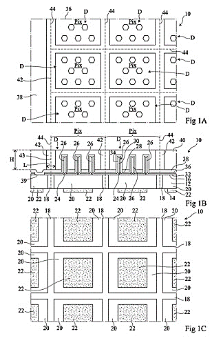
Figure 1: (Aledia’s patent EP3479408) Three-dimensional LED device with pixels of improved contrast and brightness. Each light-emitting diode comprises at least one wire, conical or frustoconical semiconductor element, integrating or covered at the top and/or at least over part of its lateral faces by a shell comprising at least one active layer designed to provide most of the radiation from the light-emitting diode. The patent has just been granted to Aledia in Europe (August 2020) and is still pending in the USA, China, Japan and Korea.
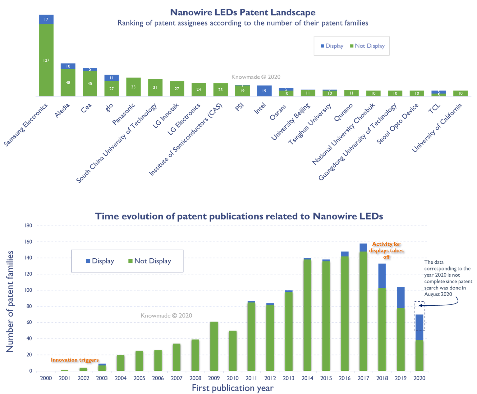
Figure 2: (a) Aledia’s main competitors in the Nanowire LED patent landscape (b) Timeline of publications in the Nanowire LED patent landscape
Another component of Aledia’s strategic move towards display applications is that Intel joined the rank of investors in 2018. At the same time, the US company was identified by Knowmade as a new entrant in the Nanowire LED patent landscape (Figure 1), with a relatively similar approach to Aledia (Figure 3) and a strong focus on micro-LED displays (Figure 2a). “Intel is developing manufacturing approaches for micro-LED structures and displays based on the assembly of nanowires, including GaN nanowires, on Si substrates,” explains Remi Comyn. Indeed, Knowmade has identified 19 inventions from Intel in the Nanowire LED patent landscape, mostly filed in the USA. As of September 2020, 5 US patents have already been granted to Intel.
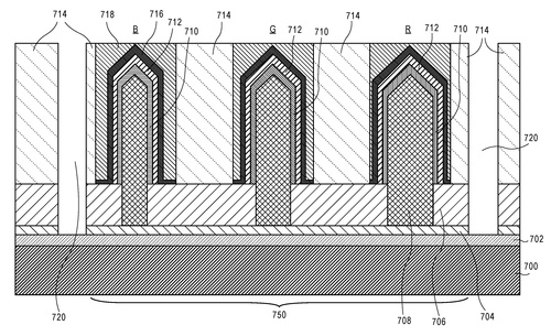
Figure 3: (Intel’s patent US 10,439,101) Micro-LED displays developed by Intel, including three different color nanowire LEDs, in particular a red-emitting diode structure (610-630 nm) comprising for instance a GaN nanowire above a Si substrate, an In0.2Ga0.8N shell layer on the GaN nanowire, an In0.4Ga0.6N active layer and a cladding layer on the InGaN active layer, the cladding layer comprising p-type GaN or p-type ZnO. The patent is granted in the USA and still pending in China and Japan.
In 2020, Knowmade investigated the GaN-on-Silicon Patent Landscape, in which Aledia owns 30 patent families. “Aledia’s inventions included in the GaN-on-Silicon patent landscape are mainly related to the growth of the nanowire emitters in large quantities with a high degree of precision and control,” affirms Remi Comyn. Additional inventions concern the fabrication of electrical contacts on GaN nanostructures (US9991342, US10340138), and device manufacturing issues (e.g. dry etching US20190172970), the removal of defective nanowires (US9299882), the monolithic integration of LEDs with devices such as transistors to control the nanowire LEDs (US10050080) or to detect the LED temperature (US20160197064). In addition, more and more display-related inventions have been identified in the GaN-on-Silicon corpus lately (e.g. US10734442, Figure 4).
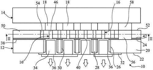
Figure 4: (Aledia’s patent US 10,734,442) The invention presents a nanowire or microwire-based LED structure enabling the reduction of crosstalk between adjacent subpixels, the enhancement of contrast and the fabrication of sub-pixels with a lateral dimension less than 15 µm. The invention has been granted to Aledia in France (2019) and the USA (August 2020) but is still pending in China, Japan, Korea, and Taiwan.
Furthermore, Aledia can rely on additional patents from its R&D partner Cea-Leti, which is well-established in nanowire LEDs and GaN-on-Silicon for optoelectronics. The institute owns 50 patent families related to nanowire LEDs with more than 170 patents granted in the US (40+), Europe (30+), China (15) and Japan (15). Interestingly, at least 5 inventions focus on displays (e.g. US8890111). Also, 19 of these inventions belong to the GaN-on-Silicon for optoelectronics patent landscape, where Cea is a well-established player (30+ inventions). Overall, between its own patents and IP agreements with partners, Aledia benefits from a strong patent portfolio of more than 170 patent families to protect the features of its technology in view of commercialization. In conclusion, major endeavors in R&D over the last three years to improve the nanowire LED technology for displays, together with its global IP strategy, have put Aledia in a good position to face the tough competition in an emerging micro-LED display market.
More patent landscape reports about Photonics, lighting or display technologies.
Press contact
contact@knowmade.fr
Le Drakkar, 2405 route des Dolines, 06560 Valbonne Sophia Antipolis, France
www.knowmade.com
About our analysts
Rémi Comyn, PhD, Rémi works for Knowmade in the field of Compound Semiconductors and Electronics. He holds a PhD in Physics from the University of Nice Sophia-Antipolis (France) in partnership with CRHEA-CNRS (Sophia-Antipolis, France) and the University of Sherbrooke (Québec, Canada). Rémi previously worked in compound semiconductors research laboratory as Research Engineer.
About Knowmade
Knowmade is a Technology Intelligence and IP Strategy consulting company specialized in analysis of patents and scientific information. The company helps innovative companies and R&D organizations to understand their competitive landscape, follow technology trends, and find out opportunities and threats in terms of technology and patents.
Knowmade’s analysts combine their strong technology expertise and in-depth knowledge of patents with powerful analytics tools and methodologies to turn patents and scientific information into business-oriented report for decision makers working in R&D, Innovation Strategy, Intellectual Property, and Marketing. Our experts provide prior art search, patent landscape analysis, scientific literature analysis, patent valuation, IP due diligence and freedom-to-operate analysis. In parallel the company proposes litigation/licensing support, technology scouting and IP/technology watch service.
Knowmade has a solid expertise in Compound Semiconductors, Power Electronics, Batteries, RF Technologies & Wireless Communications, Solid-State Lighting & Display, Photonics, Memories, MEMS & Solid-State Sensors/Actuators, Semiconductor Manufacturing, Packaging & Assembly, Medical Devices, Medical Imaging, Microfluidics, Biotechnology, Pharmaceutics, and Agri-Food.