SOPHIA ANTIPOLIS, France – February 24, 2020 | As announced earlier this month, STMicroelectronics (ST) will collaborate with Taiwan Semiconductor Manufacturing Corporation (TSMC) in order to accelerate the development of GaN technology for power applications, and more specifically for automotive applications (converters and chargers for hybrid and electric vehicles).
With this recent manufacturing partnership, STMicroelectronics has joined the row of companies which trusted TSMC for volume production of GaN power devices, including a market leader GaN Systems as well as VisIC and Navitas Semiconductor focusing on GaN power IC technology. According to the announcement, STMicroelectronics will start sampling discrete GaN power devices, which will soon be followed by GaN IC products based on TSMC’s GaN-on-Si process technology.
TSMC’s GaN-on-Si technology was reviewed in Knowmade’s GaN-on-Si Patent Landscape Analysis released in January 2020. It holds about 40 patent families (inventions) related to this technology, which regroup more than 130 patents filed worldwide, mainly in US (70+) and China (25+).
“TSMC has leading GaN-on-Silicon manufacturing expertise and we have identified at least 12 key inventions narrowly related to power applications” affirms Remi Comyn, PhD, Technology and Patent Analyst Compound Semiconductors and Electronics at Knowmade. Indeed, TSMC was actively filing GaN-on-Si patents for power applications between 2012 and 2017 and has strongly focused on US area (20+ granted patents).
The patent portfolio protects technological approaches providing improved GaN-on-Si buffer resistivity, using three main approaches:
• p-type conductivity dopants in graded buffer layers and ungraded buffer layers (patent US 8,791,504)
• diffusion blocking layer between the buffer layer and the silicon substrate (patent US 9,245,991)
• multi-strained superlattice structures (SLS) to overcome the limitations due to carbon-doping of the buffer layers (patent US 10,109,736)
Next, TSMC focused its patenting activity on removing the breakdown voltage limitations due to the surface gate-drain region, inserting buried dielectric portions in the AlGaN barrier (Figure 1a), in addition to the use of field plate structures (Figure 1b) and AlGaN barrier with Al-graded compositions (patent US 10,522,532).
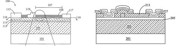
Figure 1: (a) GaN-HEMT having one or more dielectric plug portions in the barrier between the gate and the drain (patent US 8,884,308), (b) Substrate breakdown voltage improvement for group III-nitride on a silicon substrate (patent US 9,111,904).
Interestingly, the latest TSMC’s GaN-on-Si developments for power applications focused on the fabrication of GaN power integrated circuits (IC) with patent US 9,793,389 related to the isolation of adjacent GaN-on-Si power devices, and US patent 10,522,532 related to the formation of through-GaN vias (TGV).
In the GaN-on-Si Patent Landscape Analysis, Knowmade also analyzed the patent portfolio of STMicroelectronics, which is still strengthening its IP position in the power GaN patent landscape. In 2017-2018, STMicroelectronics focused on GaN device technology, especially normally-off transistor structures (Figure 2).
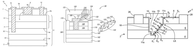
Figure 2: Normally-off structures patented in 2017-2018 by STMicroelectronics (patent US 10,566,450, US 10,050,136 and US 10,522,646).
STMicroelectronics’ normally-off transistor structures (patents US 10,516,041, US 10,566,450 and US 10,522,646) are based on a tri-layer epitaxial stack NiO/AlGaN/GaN, the selective removal of NiO in the gate region and the deposition of a gate dielectric (AlN, Al2O3 or SiO2) on the AlGaN barrier (with or without recess). The buffer region may include a first carbon-doped buffer layer for increasing the breakdown voltage and a second p-type buffer layer for limiting the degradation of dynamic on-resistance due to the first buffer layer. It can be combined with the presence of a sloped field plate in order to further reduce dynamic on-resistance phenomenon, implemented with the advantageous method described in patent US 10,050,136.
Previously – in 2018 – STMicroelectronics started a joint R&D program with The French Alternative Energies and Atomic Energy Commission (CEA), focused on the development of GaN power devices on 200-mm Silicon substrates, in view of establishing a pilot manufacturing line in 2020 in the STMicroelectronics’ foundry located in Tours, France.
CEA is also a well-established IP player in the GaN-on-Silicon patent landscape with more than 40 patented inventions. Over the last three years, it has intensified its GaN-on-Silicon patenting activity in the field of power applications with six additional inventions. CEA first focused on enhancement-mode device technology (Figure 3a), and then focused on the epi-structures in order to enhance the vertical breakdown voltage. Its recent GaN-on-Si patenting activity also includes an IP collaboration with an automotive player, Renault, regarding power GaN device technology (Figure 3b).
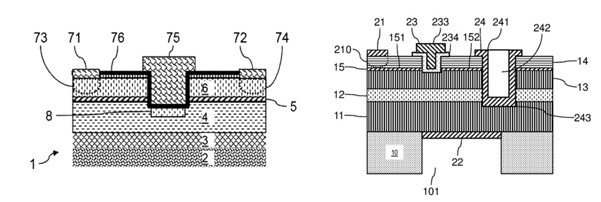
Figure 3: (a) Method for forming an implanted area under the gate region, for normally-off heterojunction transistor (patent US 10,164,081) (b) III-N heterojunction transistor with a vertical structure (WO patent application 2018/100262).
“Following the R&D collaboration between STMicroelectronics and CEA since 2018, and the recent announcement of partnership between STMicroelectronics and TSMC, we expect an acceleration of their respective patenting activity on Power GaN-on-Silicon in the next months” says Remi Comyn from Knowmade. In order to help its customers to monitor in real time the latest IP activity from competitors in the field, Knowmade has developed a dedicated GaN Power & RF patent monitoring service. The new service includes monthly updates, quarterly reports providing in-depth analysis and access to an IP analyst on request.
KnowMade’s related patent reports on power electronics technologies.
Press contact
contact@knowmade.fr
Le Drakkar, 2405 route des Dolines, 06560 Valbonne Sophia Antipolis, France
www.knowmade.com
About our analyst
Rémi Comyn, PhD, Rémi works for Knowmade in the field of Compound Semiconductors and Electronics. He holds a PhD in Physics from the University of Nice Sophia-Antipolis (France) in partnership with CRHEA-CNRS (Sophia-Antipolis, France) and the University of Sherbrooke (Québec, Canada). Rémi previously worked in compound semiconductors research laboratory as Research Engineer.
About Knowmade
Knowmade is a Technology Intelligence and IP Strategy consulting company specialized in analysis of patents and scientific information. The company helps innovative companies and R&D organizations to understand their competitive landscape, follow technology trends, and find out opportunities and threats in terms of technology and patents.
Knowmade’s analysts combine their strong technology expertise and in-depth knowledge of patents with powerful analytics tools and methodologies to turn patents and scientific information into business-oriented report for decision makers working in R&D, Innovation Strategy, Intellectual Property, and Marketing. Our experts provide prior art search, patent landscape analysis, scientific literature analysis, patent valuation, IP due diligence and freedom-to-operate analysis. In parallel the company proposes litigation/licensing support, technology scouting and IP/technology watch service.
Knowmade has a solid expertise in Compound Semiconductors, Power Electronics, Batteries, RF Technologies & Wireless Communications, Solid-State Lighting & Display, Photonics, Memories, MEMS & Solid-State Sensors/Actuators, Semiconductor Manufacturing, Packaging & Assembly, Medical Devices, Medical Imaging, Microfluidics, Biotechnology, Pharmaceutics, and Agri-Food.