SOPHIA ANTIPOLIS, France – May 19, 2026 │ KnowMade is pleased to announce the latest update of its monthly GaN research, technology, and patent landscape monitoring. New scientific breakthroughs, patent activity and industrial announcements confirm GaN is becoming a strategic semiconductor platform across computing, communications, energy and defense applications.
The global gallium nitride (GaN) ecosystem continues to gain momentum as the technology moves deeper into mainstream semiconductor roadmaps. The latest monthly R&D activity tracked by KnowMade highlights an industry rapidly evolving beyond its historical positioning in LEDs and RF power devices toward a much broader role spanning AI datacenters, optical interconnects, advanced displays, high-voltage power conversion and next-generation communication systems.
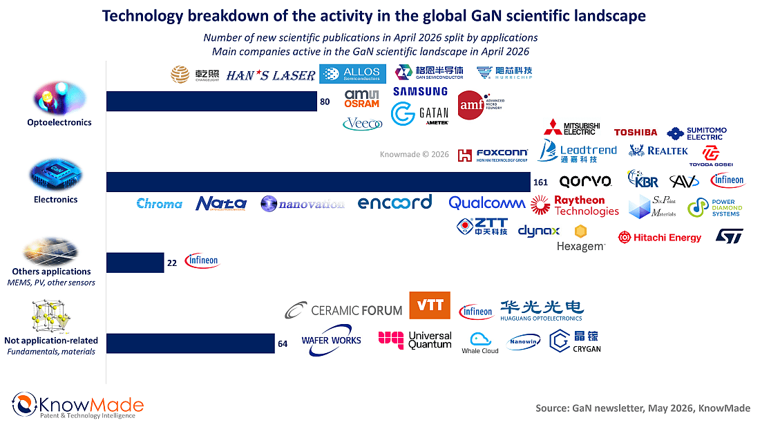
Figure 1: Application Breakdown of GaN Scientific Publications in April 2026 and leading industrial players
During the month, the GaN landscape generated more than 327 new scientific publications and 362 new patent publications worldwide, illustrating the growing intensity of both academic research and industrial competition. Electronics applications accounted for the largest share of activity, with 162 scientific papers and 238 patents, while optoelectronics remained highly dynamic with 80 scientific articles and 99 patent filings.
The latest developments confirm a major shift in the GaN industry: the question is no longer whether GaN can outperform conventional silicon technologies in specific niches, but how rapidly companies can industrialize and scale GaN-based architectures for strategic markets including AI infrastructure, electric mobility, advanced photonics and defense electronics.
Optoelectronics: microLEDs move beyond displays
One of the strongest trends observed this month is the transformation of microLED technologies from display-oriented devices into enabling platforms for photonics, AI communications and emerging computing architectures.
Recent scientific publications show how III-nitride optoelectronics are expanding into fields such as visible-light photonics, deep-UV sensing, and neurotechnology. Researchers from Toyohashi University of Technology, Meijo University, Dokkyo Medical University and ALLOS Semiconductors demonstrated a flexible InGaN microLED-electrocorticography platform capable of simultaneous neural stimulation and recording. The work illustrates how GaN microLEDs are increasingly being considered for biomedical interfaces and next-generation neuroelectronics.
At the same time, collaborations between the Max Planck Institute of Microstructure Physics, the University of Toronto, Advanced Micro Foundry and ams OSRAM demonstrated highly efficient hybrid integration of InGaN laser diodes onto silicon photonics platforms. The significance of this work lies not only in optical performance, but also in its compatibility with scalable semiconductor manufacturing processes — a key requirement for future applications in quantum photonics, biosensing and AR/VR systems.
Display technologies also remain a major focus area. A broad collaboration involving Samsung Electronics, Nagoya University and Veeco Instruments investigated efficiency mechanisms in red InGaN microLEDs, providing important insight into one of the major bottlenecks limiting fully integrated RGB microLED displays. Meanwhile, deep-UV LED research from the University of Cambridge, TU Berlin and the University of Strathclyde addressed defect-control strategies aimed at improving efficiency and lifetime in AlGaN UV emitters for sterilization and sensing applications.
Patent activity confirms that the race toward scalable microLED manufacturing is intensifying. Companies including Lumileds, Samsung Display, Silanna UV Technologies and Jade Bird Display are targeting critical challenges such as monolithic RGB integration, optical confinement, carrier management and color conversion architectures. The common objective across these patent filings is clear: simplifying manufacturing while improving optical performance and scalability for future AR/VR systems, automotive lighting and advanced displays.
At the industrial level, the most important development is the growing convergence between microLED technologies and AI infrastructure. Announcements from CEA-Leti, Mojo Vision and Avicena all point toward the same strategic direction: replacing conventional electrical interconnects with optical communication links capable of supporting future AI computing densities.
As AI accelerators become increasingly power-intensive, copper interconnects are approaching physical and thermal limitations. MicroLED technologies are now being positioned as potential low-power alternatives for short-reach optical communication inside AI servers and chiplet architectures. Mojo Vision continues to promote dense microLED optical I/O systems, while Avicena launched one of the first commercially available evaluation platforms for microLED optical interconnects, signaling that the technology is moving closer to ecosystem validation and potential deployment.
At the same time, companies such as Aledia, Polar Light Technologies and Porotech are focusing on solving one of the most critical barriers in microLED displays: scalable RGB integration and high-efficiency red emission. These challenges remain central to the commercialization of AR glasses, microdisplays and next-generation premium displays.
Electronics: GaN targets AI power, high-voltage systems and RF integration
The electronics segment of the GaN ecosystem continues to evolve rapidly as companies and research organizations push the technology toward higher voltages, higher switching frequencies and greater levels of system integration.
Recent scientific publications demonstrate significant progress in vertical power architectures, RF devices and heterostructure engineering. Researchers from Université de Tours and STMicroelectronics improved pseudo-vertical GaN p-i-n diodes for RF switching applications, while collaborations involving Linköping University, Hexagem AB, Lund University and Hitachi Energy demonstrated normally-off vertical GaN FinFETs capable of stable operation at elevated temperatures.
Several publications also highlighted the increasing maturity of vertical GaN architectures. Researchers from Ohio State University and SixPoint Materials demonstrated vertical GaN-on-GaN PN diodes exceeding 10 kV breakdown voltage, an important milestone for future medium- and high-voltage power conversion systems. Meanwhile, researchers from Universiti Sains Malaysia, Waseda University and Power Diamond Systems proposed integrated CAVET-HEMT architectures combining vertical and lateral transistor concepts in a single monolithic structure.
At the materials level, Toshiba identified previously unreported defect mechanisms in AlGaN-on-silicon structures that strongly impact leakage and manufacturing yield, underlining how defect engineering remains one of the key industrial challenges for large-scale GaN-on-Si manufacturing. In parallel, Tokyo University of Science and Sumitomo Electric Industries demonstrated high-density ScAlN/GaN heterostructures produced through sputter epitaxy, suggesting potential lower-cost pathways for future high-performance HEMTs.
Patent activity further confirms that the GaN electronics industry is entering a more mature phase focused on reliability, electrostatic control and harsh-environment operation. Infineon Technologies is working on dynamic substrate biasing techniques aimed at improving switching robustness and leakage control in GaN HEMTs. Efficient Power Conversion (EPC) is addressing threshold-voltage stability in enhancement-mode GaN transistors, while Raytheon is developing radiation-tolerant GaN heterostructures for aerospace and defense electronics.
At the same time, organizations such as Sumitomo Electric Industries and the University of Wisconsin are exploring ferroelectric-assisted GaN architectures and ScAlN heterostructures that could eventually enable multifunctional electronic devices combining RF amplification, memory behavior and tunable electronic properties.
AI infrastructure has become a major growth driver for GaN
One of the clearest themes emerging this month is the growing role of GaN technologies inside AI infrastructure and advanced datacenter architectures.
Several major announcements illustrate how AI is reshaping power electronics requirements. Enphase Energy unveiled its IQ Solid-State Transformer platform designed around distributed GaN-based power conversion for future AI datacenters. The company aims to replace traditional centralized power architectures with software-defined distributed GaN modules operating directly on emerging 800 VDC systems.
The stakes are considerable. AI servers are rapidly approaching megawatt-scale rack densities, creating unprecedented challenges in power delivery, thermal management and energy efficiency. GaN technologies are increasingly being viewed as one of the few semiconductor platforms capable of supporting the switching speeds, power density and compact form factors required by future AI infrastructure.
Intel Foundry’s announcement of ultra-thin 300 mm GaN chiplets with integrated digital logic reinforces this trend. Intel is positioning GaN not as a standalone discrete technology, but as part of the future chiplet ecosystem for AI processors and advanced computing systems. By integrating digital control directly onto GaN devices using scalable 300 mm manufacturing processes, Intel is effectively pushing GaN toward highly integrated intelligent power architectures.
Meanwhile, NexGen Power Systems continues promoting vertical GaN as a potential long-term alternative to both silicon and silicon carbide for ultra-high-density power conversion. Its communications emphasize multi-kilovolt capability, MHz-class switching and improved avalanche robustness, targeting applications ranging from EVs to AI infrastructure and industrial electrification.
The rapid expansion of GaN markets is also putting increasing attention on supply-chain readiness and manufacturing scalability. South Korean epiwafer supplier IVWorks raised new funding to industrialize its proprietary reGaN technology for RF and AI power semiconductor applications, highlighting how epitaxy and wafer engineering are becoming strategic assets within the GaN ecosystem. The announcement comes as IDTechEx forecasts strong long-term adoption of GaN technologies across AI datacenters, electric vehicles and renewable-energy systems, reinforcing expectations of significant growth in demand for advanced GaN materials and device platforms.
Strategic competition and geopolitics reshape the GaN landscape
As GaN technologies become increasingly strategic for AI infrastructure, automotive power electronics, telecom and defense systems, competition is extending far beyond device performance and manufacturing scale. Intellectual property, supply-chain positioning and geopolitical alignment are now becoming major factors shaping the future structure of the GaN industry.
This evolution is clearly illustrated by the escalating patent dispute between Infineon Technologies and Chinese GaN supplier Innoscience. A recent ruling by the US International Trade Commission intensified the rivalry by imposing restrictions on certain Innoscience products in the US market. However, the broader significance of the conflict goes well beyond the legal outcome itself. The case highlights how GaN is becoming entangled in the wider geopolitical fragmentation of the semiconductor industry. While Infineon presented the decision as a major intellectual-property victory, Innoscience responded that the products concerned had already been redesigned or phased out, allowing the company to continue shipping newer-generation devices. The situation illustrates how rapidly evolving GaN product cycles can complicate the practical enforcement of patent restrictions.
More importantly, the dispute reflects growing concerns around supply-chain sovereignty and what many Western customers now describe as “red supply chains.” These concerns are particularly acute in AI infrastructure and hyperscale datacenters, where sourcing decisions are increasingly influenced not only by technical performance and cost, but also by geopolitical risk. Although Innoscience has successfully entered parts of Nvidia’s ecosystem, much of its activity reportedly remains concentrated within China-focused deployments rather than global AI infrastructure programs.
At the same time, the competitive pressure coming from Chinese GaN suppliers is beginning to reshape the broader industry landscape. Aggressive pricing strategies and rapid capacity expansion are contributing to major supply-chain adjustments across Asia. Recent decisions by companies such as TSMC to step back from parts of the GaN foundry business, alongside new investments from Powerchip Semiconductor Manufacturing Corporation and other foundries, illustrate how quickly the global GaN manufacturing ecosystem is reorganizing itself.
These developments confirm that GaN is no longer viewed simply as an emerging semiconductor technology. It is increasingly becoming a strategic industry where technological leadership, manufacturing control, intellectual property and geopolitical alignment are all deeply interconnected.
About the GaN Monthly Newsletter
KnowMade’s monthly GaN newsletter provides continuous monitoring and analysis of scientific publications, patent activity and industrial developments across the global gallium nitride ecosystem. It is best suited for researchers, engineers, and IP professionals who want to monitor the latest research findings, scientific collaborations, R&D and patenting activities, emerging technologies and applications, and the competitive landscape. This monitoring service covers both optoelectronics and electronics applications, including microLEDs, photonics, RF devices, power electronics, AI infrastructure, automotive systems and defense technologies.
Press contact
contact@knowmade.fr
Le Drakkar, 2405 route des Dolines, 06560 Valbonne Sophia Antipolis, France
www.knowmade.com
About KnowMade
KnowMade is a technology intelligence and IP strategy firm specializing in the analysis of patents and scientific publications. We assist innovative companies, investors, and research organizations in understanding the competitive landscape, anticipating technological trends, identifying opportunities and risks, improving their R&D, and shaping effective IP strategies.
KnowMade’s analysts combine their strong technology expertise and in-depth knowledge of patents with powerful analytics tools and methodologies to transform patent and scientific data into actionable insights to support decision-making in R&D, innovation, investment, and intellectual property.
KnowMade has solid expertise in Semiconductors and Packaging, Power Electronics, Batteries and Energy Management, RF and Wireless Communications, Photonics, MEMS, Sensing and Imaging, Medical Devices, Biotechnology, Pharmaceuticals, and Agri-Food.