SOPHIA ANTIPOLIS, France – August 02, 2022 │ The French patent analysis firm KnowMade is launching a series on Toyota’s patent activity – stay tuned to see its R&D strategy unveiled:
- Hydrogen-based Fuel Cell Electric Vehicles: a winning bet for Toyota?
- Toyota’s triptych IP strategy on batteries to conquer the EV market
- Toyota Group, a leading IP player in the development of sensors and autonomous vehicles technologies
Toyota’s business strategy towards decarbonization: a mix of HEV, FCEV and… BEV
Until recently, Toyota was seen as a hybrid and fuel-cell oriented automaker. The Japanese automaker successfully commercialized its self-charging hybrid technology in 1997, resulting in the sale of more than 15 million hybrid electric vehicles (HEV). In contrast, after the commercial failure in 2014 of the second generation of its RAV4 electric vehicle (EV) model, developed with Tesla and commercialized in California only, Toyota seemed reluctant to move into purely battery-powered electric vehicles (BEV) in the short or medium term, according to repeated public statements from its executives. Since 2014, Toyota has instead highlighted its continuous development in the field of hydrogen-powered fuel cell electric vehicles (FCEV), where it took the leadership with its models Mirai I (2014) and Mirai II (2020).
However, the first articles from KnowMade’s Toyota patent portfolio analysis series indicate that Toyota group has been at the forefront of the development of both BEV and FCEV technologies. Over the last decade, Toyota group published 400 to 600 fuel cell inventions per year, and about 1,200 battery inventions per year, which positions Toyota group as a top innovator in the field of EV technology. Innovation leadership in batteries, electric motors and power electronics, often considered as the “three enabling technologies” for BEV, is actually commonly cited as the main reason behind the success of Tesla, the top BEV manufacturer as of 2022.
EV technology driving major innovations in power electronics
A revolution began in 2018 when Tesla chose to replace the incumbent IGBT technology in its Model 3, based on mainstream Si technology, by the emerging silicon carbide (SiC) MOSFET technology. The new SiC devices have been implemented in one of the most critical parts of the car – the main inverter – which controls the electric motor, indicating the high level of confidence Tesla has in the technology. SiC MOSFET technology provides many advantages over Si IGBT technology at system level, because silicon carbide devices can operate efficiently at high switching speed and high temperature. As demonstrated in Tesla’s EV inverter, by taking advantage of these superior device features, the weight of the system can be significantly reduced, due to the smaller size of passive components and lower cooling requirements, while enhancing system efficiency. Accordingly, the package of SiC power modules needs to keep up with higher power densities and higher switching frequencies, spurring the development of new technologies to address issues related to heat dissipation, parasitic inductances, etc. For instance, Tesla implemented Ag sintering for die attach in its SiC power modules, enabling enhanced thermal and electrical conductivities, as well as better thermal reliability, compared to conventional solders. Furthermore, Tesla opted for copper leadframes to handle larger power densities between silicon carbide power devices inside the module. Following Tesla’s lead, multiple car makers decided to adopt SiC technology in their BEV platforms, including Hyundai Motor, BYD, Volkswagen group and GM. More recently, as a first step into silicon carbide technology, Toyota announced the integration of SiC devices in the intelligent power modules (IPM) used for its second-generation Mirai FCEV. The lateness of this announcement contrasts with Toyota SiC patenting activity, which indicates that Toyota group has actually been engaged for more than two decades in the development of SiC technology for EV applications.
Patent analysis reveals Toyota’s innovation strategy in power electronics to prepare for mass adoption of EV
KnowMade specializes in the analysis of the patenting activity (patent filings) of players to provide a better understanding of their market, innovation and intellectual property (IP) strategies. The level of patenting activity often reflects the level of R&D investment made by a company in a technology. Furthermore, patent analysis can provide clues as to the technology readiness level reached by the company. Finally, the technology coverage along the value chain and the geographical coverage of the patent portfolios are closely related to the business strategy of the company.
In this article, we leverage KnowMade’s know-how in patent analysis to describe Toyota’s innovation strategy in the field of power chips and power modules, focusing on SiC technology as a must-have technology for the next generations of EV.
Toyota Motor and Denso: A strong synergy between two pioneers of SiC technology
Looking at their patenting activities, several members of the Toyota Group have been actively developing silicon carbide technology over the last few decades, including Toyota Motor, Denso, Toyota Central Research and Development Laboratory (Toyota CRDL), Toyota Industries and Toyota Tsusho. In our latest SiC power patent landscape, the main entities filing SiC patents in Toyota Group are Denso (800+ inventions), Toyota Motor (510+) and Toyota CRDL (170+).
Denso pioneered power SiC technology and started filing numerous SiC patents in the late 1990s, focusing on SiC substrates and SiC devices. Toyota Motor was also a pioneer for power silicon carbide technology with its first patent filings back in the early 1990s. However, its patenting activity really took off in the mid-2000s, and further accelerated in 2010/2011, focusing on SiC substrates and SiC devices as well. Since then, the level of patenting activity related to SiC technology from Denso and Toyota has remained high, featuring a combined total of more than 50 new inventions per year
(Figure 1).
As mentioned before, the patenting activity of Denso and Toyota was focused on SiC substrates and SiC devices until 2016. The number of SiC power module patents then sharply increased in 2016 and peaked in 2019, with more than 30 new SiC power module publications. Overall, relatively few Toyota SiC circuit patents have been published so far and most of them have been filed by Denso. Notably, Toyota Motor and Virginia Tech collaborated on SiC circuits, leading to the co-filing of at least eight new patent families (inventions) between 2015 and 2017.
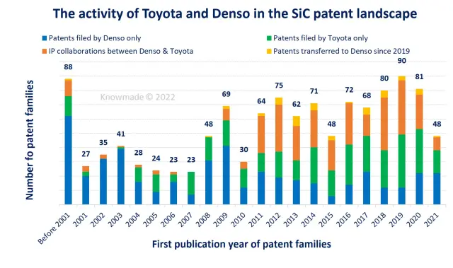
Fig. 1: Patenting activity of Toyota Group (patents published up to August 2021).
In the field of power silicon carbide technology, there has been a very close IP cooperation between Denso and Toyota Motor/Toyota CRDL, which strengthened in 2010/2011. The number of co-filings has remained high over the whole last decade, translating to more than 320 patent co-filings since the early 2000s (Figure 2). Overall, IP collaborations and IP transfers with Denso account for more than half of Toyota’s patenting activity in the power SiC patent landscape. The IP collaboration focuses on SiC power devices (203+ common inventions) and SiC substrates (80+), especially SiC MOSFET (180+) and bulk SiC (60+).
Denso taking over the leadership in SiC technology for EV
In 2018, Toyota Motor and Denso agreed to consolidate mass-production development and production of both Toyota and Denso within Denso. In doing so, Toyota Motor aimed to free up resources to compete more effectively on new vehicle technologies (electric cars, self-driving vehicles, ride-sharing and other mobility services). In July 2019, Denso and Toyota Motor agreed to establish a joint venture for research and advanced development of next-generation, in-vehicle semiconductors: MIRISE Technologies (Denso: 51%, Toyota: 49%). MIRISE works on three technology development fields: (1) power electronics, (2) sensing and (3) SoC (System-on-a-Chip). As of June 2022, six patent families (inventions) have been assigned to MIRISE Technologies, among which one co-filing with Denso, Toyota Motor and Disco (Japanese manufacturer of processing equipment and tooling). The patent co-filing describes a process related to SiC dicing.
As Toyota and Denso were consolidating their collaboration at both development and production levels, starting MIRISE joint venture, Toyota transferred the IP rights of about 40 Toyota silicon carbide patents to Denso in the last three years. This further confirms that Toyota is transferring the leadership to Denso to develop SiC technology up to its integration into EV. The IP rights transferred by Toyota Motor/Toyota CRDL to Denso mainly relate to SiC power modules (22 inventions) and SiC power devices (17 inventions). Accordingly, these IP transfers highlight key patents in the eyes of Toyota and Denso for the development of SiC technology in EV applications.
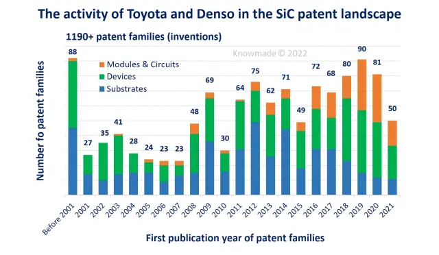
Fig. 2: Patenting activity including IP collaborations and IP transfers between Toyota and Denso (patents published up to August 2021).
A large IP portfolio to cover SiC crystal growth, SiC wafering and SiC epitaxial wafers
In the field of bulk SiC, Denso and Toyota Motor position themselves as strong innovators. Both companies developed the physical vapor transport (PVT) technology for bulk SiC crystal growth, which is the best-established technology in the SiC wafer industry (used by II-VI, Wolfspeed and SiCrystal for example).
Furthermore, Denso is the main IP player engaged in the development of chemical vapor deposition (CVD) growth for bulk SiC (60+ patents). This technique has also been developed by Norstel (now STMicroelectronics Silicon Carbide AB), the only manufacturer commercially growing SiC bulk crystals from gases. Denso filed two recent patent applications related to CVD for bulk SiC growth. The first application deals with the distribution of dislocations along the wafer diameter. The second application relates to a CVD growth apparatus which reduces the probability of occurrence of heterogeneous polymorphism or a differently oriented crystal in the facet plane of the SiC single crystal.
Recent IP collaborators of Denso include LPE (Italy) for CVD growth equipment, CRIEPI (Japan) to reduce dislocations in bulk SiC and Showa Denko (Japan) to suppress the occurrence of basal plane dislocations in bulk SiC. In 2020, Denso announced that it would adopt Showa Denko’s SiC epitaxial wafers (150mm-diameter) for the production of SiC power devices. Showa Denko combines strong leadership in the SiC substrate IP battlefield with a leading position in the global market of SiC epiwafers. Our previous article detailed its IP strategy to consolidate its activities related to SiC bare and epitaxial wafers.
On the other hand, Toyota leads the IP activity related to solution growth (a promising technology not yet at the commercial stage). With more than 150 related inventions, Toyota stands far ahead of its main IP competitors LG Chem (an IP newcomer) and Kyocera (an established IP player no longer active), patenting solution growth apparatuses and methods to produce SiC bulk crystals.
Alternatively, Toyota Tsusho is developing an innovative approach with Kwansei Gakuin University (Japan) to remove sub-surface damage induced by mechanical processing, such as scratches, from SiC wafers, and create a defect-free buffer layer suitable for CVD growth of SiC epitaxial structures. The collaboration has resulted in at least 17 patent co-filings since 2019.
Finally, more than 80 patents refer to SiC epiwafers, of which 50 inventions focused on CVD epitaxy. Apart from the IP collaboration with Kwansei Gakuin University, very few SiC epitaxial wafer inventions were filed recently by Denso and Toyota.
Acceleration in the joint development of trench SiC MOSFET for EV applications
Before 2010, most SiC MOSFET patents were filed by Denso on both planar and trench SiC MOSFET (Figure 3). The trench design provides several benefits for the performance of SiC MOSFET, such as lower on-resistance, smaller parasitic capacitance, and improved switching performance. As a result, converter losses and heat sink requirements can be reduced by adopting the trench SiC MOSFETs, so the power density of EV inverters can be increased by leveraging these characteristics. In EV applications, where the total weight of power converters is very important, the trench design provides a competitive advantage compared to the planar design. Therefore, when Denso started a collaboration with Toyota Motor from 2010 to develop SiC MOSFET technology, they put the emphasis on the trench MOSFET structure, as demonstrated by their patenting activity.
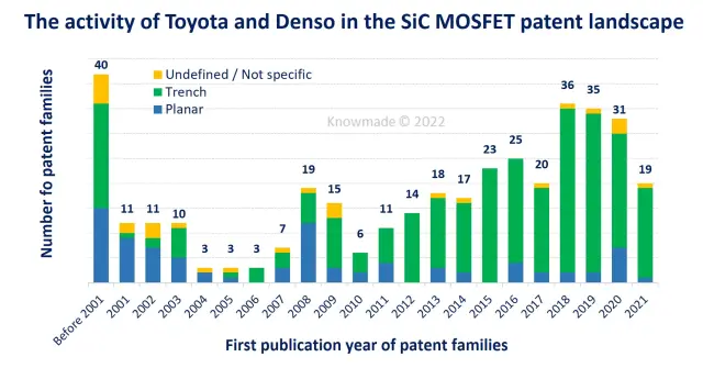
Fig. 3: The patenting activity of Toyota group in the SiC MOSFET patent landscape (patents published up to August 2021).
Denso commercialized its first silicon carbide transistor in 2014, but the company said that the new device was for audio products. It was only in 2020 that Denso released an automotive product including an in-vehicle SiC transistor integrated into a booster power module. The product was adopted by Toyota in the new Mirai model released in 2020 (Figure 4). Denso branded the SiC power technology as REVOSIC® technology and announced on-going R&D activities to expand its application to BEV. Accordingly, it seems that Denso and Toyota have been very cautious in the adoption of SiC technology for power applications, moving progressively from its integration in less critical power electronics systems to the more critical EV inverter.
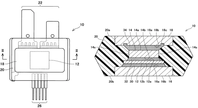
Fig. 4: Patent application filed by Denso/Toyota, illustrating the package used to integrate the new SiC REVOSIC® technology into a booster power module for FCEV. This application aims to suppress a rise of temperature at the corner of the conductive spacer 14.
The Trench SiC MOSFET structure presented by Denso consists of a deep-P encapsulated trench MOSFET structure, known as orthogonal deep-P trench MOSFET structure (ODS, Figure 5). It contrasts with conventional parallel deep-P trench MOSFET structures (PDS). MOSFET structures have a p-type region (Deep-P) under the trench, to protect the gate oxide of the trench bottom from the high electric field in the off-state. The main advantage of the novel structure presented by Denso is that independent design of trench gate pitch and JFET cell pitch is possible. As a result, trench gate pitch and JFET cell pitch of the presented structure are 34% and 64% lower than those of the conventional structure. This approach is then optimized to obtain low on-resistance, while maintaining a high breakdown voltage.
At least eight patents related to the deep-P encapsulated trench MOSFET structure have been filed by Denso and Toyota since 2017, of which 4 inventions published in the last couple of years. Other recent trench MOSFET patent applications relate to different structures or technical areas, including an edge termination region, current sense region and gate reliability (threshold stability, electrode overheating in the region near the gate dielectric film and an insulating protective film).
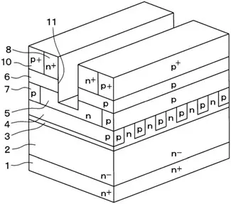
Fig. 5: Patent US10867876 filed by Denso in 2019 and describing orthogonal deep-P trench MOSFET structure (ODS).
Power modules for EV: Power card resin-molded packages with double-sided cooling (DSC) structure
Toyota and Denso hold sizeable patent portfolios for power module technology, including more than 150 patent families (inventions) explicitly applicable to silicon carbide, although few patents focus on SiC power modules. Patent portfolio analysis shows that their patenting activity covers the main technical challenges for EV applications (heat dissipation, thermal reliability, parasitic inductance, miniaturization) and technical areas (die attach, encapsulation) of power module technology. More than 50 power module patent families (inventions) have been co-filed by Toyota Motor and Denso.
Over the last few years, Toyota Motor has focused on improving the applicability of the power control unit (PCU) between different vehicle models, as well as downsizing the PCU. In order to achieve this objective, Toyota Motor has co-developed a 2-in-1 double-sided cooling (DSC) power module
(4th generation) with Denso, to replace the 1-in-1 single-sided cooling power module developed previously (3rd generation). In the latter, the transistors and diodes were mounted planarly in the single-cooling structure and, as a result, the volume used to get too large for high output vehicles.
In the DSC structure, the modules referred to as power cards consist of resin-molded packages including chips, heat sink and terminals. Most encapsulation patents filed by Toyota/Denso focused on molding encapsulation (90+ inventions). The power cards are stacked in the cooler, forming the power stack, which includes the cooler, insulating plates, thermal conductive grease, compression plate spring and spacers. As a result, the quantity of power cards is adjustable to the vehicle size (flexibility) and the volume can be reduced by more than 20%. Furthermore, the inductance between P and N terminals is reduced by more than 50% due to the elimination of wiring between the upper and lower arm.
The 2-in-1 structure is made possible by the N-structure (Figure 6) due to the greater reliability of solder joints after repetitive heat stress, good electromigration tolerance at high-current density, and other factors with respect to other structures such as the U-structure. The module is substrate-less and baseplate-less. There is no insulation in the module, power devices are bonded directly onto a copper plate, a leadframe or a heat-spreader. The insulation is achieved by an external ceramic insulating foil applying thermal grease between the module and the cooling system.
Overall, Toyota has filed more than 60 inventions related to the double-sided cooling structure and package. Focusing on the N-structure module, continuous patenting activity is observed over the last decade up to 2018. Many patents were co-filed with Denso, but few patents are specific to SiC technology (i.e., generic patents, applicable to IGBT modules or other).
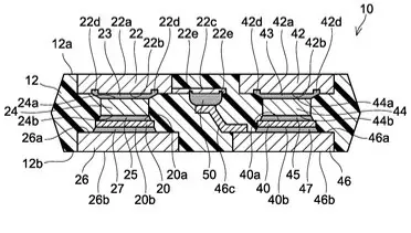
Fig. 6: Patent application US10763240 filed in 2018, describing the N-structure module.
Toyota Motor is well positioned on innovative approaches for die attach technology
Furthermore, Toyota Motor is one of the main active IP players for transient liquid phase (TLP) bonding techniques in the power module patent landscape. TLP bonding represents an alternative to conventional solder techniques and silver or copper sintering techniques for high-temperature operation. Toyota Motor started filing patents related to the TLP bonding technology in the early 2010s. Most TLP patents were transferred to Denso in 2019. A recent patent application was published in 2021 and co-filed with University of Illinois. It describes an inverse opal structure (MIO) which provides a compact bond layer that compensates for thermally-induced stress and facilitates thermal management. Another patent published in 2021, whose IP rights have already been transferred to Denso, describes electronic modules including an MIO substrate with integrated jet cooling. In contrast, few patents related to silver or copper sintering have been identified in Toyota group’s patent portfolio. The first patent families related to power modules using Ag sintering have been published recently by Denso.
Toyota group: A vertically-integrated SiC innovator steadily increasing its focus on EV applications
Back to the Tesla case study. The Californian company is considered a pioneer in the use of silicon carbide in the traction inverter but had no patent focused on SiC semiconductor technology nor power module technology as of August 2021. Instead, Tesla has had close relationships with innovators in these fields (STMicroelectronics, Boschman Advanced Packaging Technology), explaining its fast move towards SiC technology. In contrast, the analysis of Toyota group’s patent portfolio shows that the Japanese corporation has designed a strategy to internally build strong expertise all along the supply/value chain of power SiC technology. Analysis of the patent portfolio features a broad coverage of the SiC crystal growth techniques and SiC bare wafer/epiwafer technical areas, with more than 300 alive patent families. Therefore, Toyota group has significant resources internally to lift any barrier related to SiC material issues. Moving down the supply/value chain, the technical coverage of the patent portfolio narrows down, especially in the 2010s, to focus on EV applications, with more than 210 alive trench SiC MOSFET patents, and numerous patents covering card-like resin-molded power modules, and high-temperature die attach techniques.
An IP strategy securing Toyota’s future in the global competitive EV market
Although Toyota Motor and Denso identified silicon carbide as a key semiconductor in the future of power electronics early on, as demonstrated by a long history of SiC patent filings, Toyota group seems to have been a little cautious with regards to its use in the BEV inverter, starting with audio products in 2014 and booster power modules in FCEV in 2020. But the acceleration in the patenting activity related to the development of SiC trench MOSFET and SiC power modules in the 2010s, with Denso taking the lead in development and production, suggests that Toyota group is now fully engaged in the integration of SiC technology into EV platforms, including BEV inverters. Overall, Toyota group now occupies a strong IP position in the US and Japanese markets, where most of its SiC patents are granted; but its recent patenting activity indicates an endeavor to strengthen its position in other strategic markets for SiC technology, especially Europe and China. In its latest IP reports covering power SiC and power modules, KnowMade has seen this trend strengthening in the patenting activity of the main IP and market players. Although the context is now very different, the global patenting activity to support Toyota’s international business strategy should minimize the risks related to low acceptance rate from local markets and/or IP litigations, as experienced with the RAV4 EV model in past decades. What’s more, the silicon carbide technology co-developed by Toyota Motor and Denso, with Denso taking over production and development, will certainly benefit other OEMs looking for solid know-how and expertise all along the supply/value chain of EV (BEV, HEV and FCEV), from raw materials to advanced electronic systems.
Discover KnowMade’s expertise: Power electronics patent landscape reports.
Press contact
contact@knowmade.fr
Le Drakkar, 2405 route des Dolines, 06560 Valbonne Sophia Antipolis, France
www.knowmade.com
About our analyst
Rémi Comyn, PhD, Rémi works for Knowmade in the field of Compound Semiconductors and Electronics. He holds a PhD in Physics from the University of Nice Sophia-Antipolis (France) in partnership with CRHEA-CNRS (Sophia-Antipolis, France) and the University of Sherbrooke (Québec, Canada). Rémi previously worked in compound semiconductors research laboratory as Research Engineer.
About Knowmade
Knowmade is a Technology Intelligence and IP Strategy consulting company specialized in analysis of patents and scientific information. The company helps innovative companies and R&D organizations to understand their competitive landscape, follow technology trends, and find out opportunities and threats in terms of technology and patents.
Knowmade’s analysts combine their strong technology expertise and in-depth knowledge of patents with powerful analytics tools and methodologies to turn patents and scientific information into business-oriented report for decision makers working in R&D, Innovation Strategy, Intellectual Property, and Marketing. Our experts provide prior art search, patent landscape analysis, scientific literature analysis, patent valuation, IP due diligence and freedom-to-operate analysis. In parallel the company proposes litigation/licensing support, technology scouting and IP/technology watch service.
Knowmade has a solid expertise in Compound Semiconductors, Power Electronics, Batteries, RF Technologies & Wireless Communications, Solid-State Lighting & Display, Photonics, Memories, MEMS & Solid-State Sensors/Actuators, Semiconductor Manufacturing, Packaging & Assembly, Medical Devices, Medical Imaging, Microfluidics, Biotechnology, Pharmaceutics, and Agri-Food.