August 25, 2022

Semiconductors, and related microelectronics, photonics, and packaging technologies

The semiconductor industry is on the cusp of a decade of growth

KnowMade's semiconductor expertise.

The semiconductor market is expected to keep growing due to a variety of megatrends, such as digitalization of our system, 5G proliferation, increasing demand for electric vehicles (EVs), autonomous driving, augmented and virtual realities (AR/VR), and wider implementation of artificial intelligence (AI).

In the coming years, the market will be mainly driven by the automotive, computing & data storage, and wireless industries. The automotive semiconductor segment is pushed by the rising need for electrification and self-driving. On the other hand, the computation and data-storage market is driven by the requirement for servers to accommodate cloud computing and AI. In the wireless sector, it is smartphones that will primarily contribute to the growth, supported by 5G expansion. For the next decade, there are new technological prospects in the areas of power management, smart transportation, 5G/6G and IoT, next-generation computing, photonics, AI, quantum, etc.

The semiconductor industry requires long-term investments, and companies invest heavily in R&D projects, striving for innovation across all segments (memory, logic, analog, discrete, optical components, sensors,), as they know distinctive technologies and products is the key to success. Semiconductor companies must develop more sophisticated chips required for advanced computing, mobility, and connectivity applications. While some players focus on developing leading-edge chips with ever smaller node size, others are pursuing “more than Moore” innovations, which involve developing semiconductors devices based on materials other than silicon such as silicon carbide (SiC) and gallium nitride (GaN). Semiconductor packaging is now considered a critical part of semiconductor design and manufacturing, and advanced packaging (fan-out WLP, 2.5D/3D IC, hybrid bonding, chiplets, etc.) now provides a cost-effective way to combine chips at different technology nodes.

Semiconductors are a vital part of differentiating products, and the ongoing chip shortage is prompting certain electronics companies and automotive original equipment manufacturers (OEMs) to do their chip design internally to raise customization and eliminate bottlenecks. As competition increase and chip/device design and production become more intricate, it is increasingly important to better the collaborations within the semiconductor ecosystem, and some companies might pursue a merger and acquisition (M&A) strategy as the industry consolidates.

KnowMade’s purpose

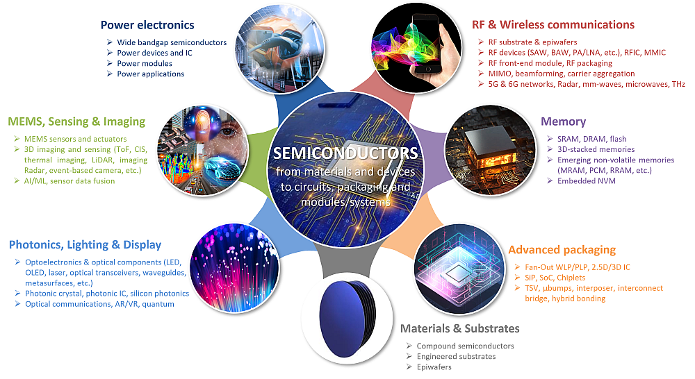
Monitoring and analyzing semiconductor and microelectronics/photonics innovations, from materials and devices to circuits, packaging, and modules/systems, is our mission. Our fields of expertise include power electronics, RF & wireless communications, MEMS technologies, sensing & imaging, photonics, lighting & display, memory, and advanced packaging.

At KnowMade, we strive to help our clients innovate and gain competitive edge they need to stay ahead of the game in technology and intellectual property (IP). Our patent and technology analysis allows us to have a better understanding of the semiconductor industry, and offer our expertise to identify, analyze and track technological innovations, key players and new entrants, as well as their technology roadmap and IP strategy. We also use these insights to spot any potential IP/technology risks or opportunities. We offer a variety of products and services related to the semiconductor field, comprising patent reports, monitors, and customized studies that are designed to meet your needs and budget.

We provide services to a wide range of entities within the semiconductor industry, from material/equipment suppliers and wafer/epiwafer providers, to integrated device manufacturers (IDMs), fabless players, pure play foundries, outsourced semiconductor assembly and test companies (OSATs), start-ups, research organizations, and investors, of all sizes and located all over the globe. We help key decision-makers engaged in the design, manufacture, or supply of semiconductors, microelectronics, and photonics devices, as well as those involved in investing in the semiconductor industry. With the dawn of the Asian century, we are increasingly focused on understanding the implications of China’s growth for our clients’ semiconductor business.

We keep track any patent activities and technology developments related to all semiconductor segments (memory, logic, analog, discrete, optical components, sensors, etc.) and markets (consumer electronics, communication, computing and data storage, automotive electronics, industrial electronics, etc.), with a particular focus on mobility, connectivity, and computing applications.

Some areas of interest for patent analysis

At KnowMade, we give special consideration to innovations in the following areas.

Electrification

Transportation electrification and demand for energy consumption and CO2 emission reduction are an opportunity for power electronics. GaN and SiC have emerged as the most promising candidates to improve efficiency and compactness in a variety of applications such as renewables, power supplies, and transportation.

However, the large-scale adoption of GaN and SiC power electronics devices implies overcoming certain challenges such as building a complete, resilient supply chain, ensuring the performance and reliability of power electronics devices in the critical application fields, and proving cost competitiveness with other solutions at system level. Different development strategies are currently being adopted by GaN and SiC industrial players, either exploring a fabless model, a foundry model or a vertical integration model.

KnowMade’s power electronics teams monitor and analyze any patent developments across the whole value chain, from the crystal growth of bulk and epitaxial materials to the manufacturing of power electronics devices, their packaging and interconnections in sub-systems. We track the players actively engaged in the development of SiC and GaN technologies, including current market players as well as newcomers and those going under the radar. Our patent analysis provides a comprehensive picture of the current and future power electronics competitive landscape, your competitors’ latest R&D activities and roadmap, their target applications and markets.

Automotive and Mobility

Transportation is undergoing its most radical transformation with autonomous, connected, and electric vehicles. The automotive and mobility sector is using more and more semiconductor devices to achieve increased autonomy and communications capabilities. Advanced driver assistance systems (ADAS) and autonomous navigation are driving new perception systems such as LiDAR, imaging RADAR, event-based camera, and the use of sensors (CIS, MEMS, etc.), photonic/optical systems, RF modules, control/calculation chips (MCU, CPU, FPGA, AI chips, etc.), and memories.

KnowMade’s teams look at new trends and innovations coming from semiconductor and electronics devices and modules that meet mobility usage developments. Our products and services give you the ability to monitor and assess global automotive technology trends so that you can develop strategic plans, particularly focusing smart mobility, vehicle-to-everything communication (V2X), autonomy, and electric propulsion.

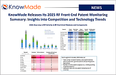
RF Technologies for 5G & Connectivity

The world is transforming to connect everyone to everything, all the time, making RF components essential for the next generation of connectivity (5G, IoT, V2X, etc.).

5G networks are expected to provide data speeds that are much faster than previous generations of mobile networks, as well as lower latency which is necessary for applications that require real-time responses, and improved reliability in communications. Semiconductors will be critical in delivering the full promise of 5G and beyond. 5G has caused a major increase in the demand for reliable, high-performance RF Front End (RFFE) solutions, the core of mobile communications.

The RF component and module industries offer plenty of growth opportunities, but the established companies are facing strong competition from China where the RFFE ecosystem is quickly developing with many emerging companies supported by the strong domestic demand.

The KnowMade RF team’s daily tasks consist of monitoring and analyzing meaningful technology trends, changes in the competitive environment, and intellectual property strategies of RF companies, covering a variety of topics ranging from RF substrates (such as SOI and POI) to RF devices (including SAW, BAW, XBAR, PA/LNA, and antennas), RF front end modules, and RF advanced packaging (such as FOWLP).

Digitalization and Next Generation Memory Technologies

Memory technology plays a vital role in enabling the digital transformation of our data-centric society, and the needs for memory chips will continue to grow, driven by soaring bit demand from (AI), cloud computing, mobility, and IoT.

High data storage density, bandwidth capability, energy consumption and cost are the critical factors on which current memory technology developments are focusing. The “memory bottleneck” is created as more and more data are transferred between processor and system memory, and new solutions are being developed to bring the data processing unit and memory unit closer together, utilizing 3D-stacked memory architecture and adopting wafer-to-wafer stacking approach (hybrid bonding) to integrate memory and logic chips (advanced IC packaging). The performances can be also improved with in-memory computing, where data are processed within the memory device. As traditional floating gate-based embedded non-volatile memory (eNVM) is becoming more complex, new memory technologies such as FeFETs, MRAM, PCM and RRAM are being heavily explored.

KnowMade’s memory activity is centered around understanding the latest technology innovations and their implementations, alongside the main players’ intellectual property (patents) strategies. The memory teams monitor and analyze any patent developments related to cutting-edge memory components (MRAM, PCM, ReRAM, etc.), new applications (neural networks, neuromorphic computing, etc.), and innovative packaging technologies (hybrid bonding, etc.).

Semiconductor Advanced Packaging

Advanced packaging group a variety of different techniques, including fan-out wafer-level packaging (FOWLP), 2.5D (interposer, interconnect bridge), 3D IC, hybrid bonding, etc. Chiplet-based design (interconnect by chip-to-chip bonding) is a new alternative solution to a system-on-a-chip (SoC) of integrating various types of dies, such as I/Os, memory and processor cores, in a package. Advanced packaging of semiconductor components allows greater number of connection points, higher data-transfer rates, better performance, and better heat management. In addition, it provides a cost-effective way to combine chips developed at different process nodes (heterogeneous integration). Packaging innovations are driven by foundries and OSATs, and they create opportunities for other players across the value chain since they support demand for new materials and equipment.

At KnowMade we provide you a unique and valuable understanding of the latest innovations and advanced packaging ecosystem evolution through patent analysis reports and monitoring services. By tracking patenting activity of leading companies such as TSMC, Samsung, Intel, Amkor, ASE/SPIL, JCET, Nepes, PTI, Deca, Huatian, TFME, SJSemi, SK Hynix, Xperi, etc. we are able to highlight their technology and IP strategy.


Latest reports on semiconductor technologies

Featured image of the LiDAR for automotive patent landscape 2025.
The global IP battlefield is heating up: who are the key players, and which technologies will shape the future of LiDAR for automotive? Publication December [...]
The global IP battlefield is heating up: who are the key players, and which technologies will shape the future of imaging radar for autonomous mobility? Publication [...]
Featured image of the Silicon Carbide Patent Lanscape 2024.
Figure out the latest IP evolutions and trends in the SiC industry. Explore the patenting activities across the SiC supply chain. Publication December 2024 Download [...]

Latest patent monitors on semiconductor technologies

Featured image of the SiC patent monitor.
Get updated data on SiC-related patent activity for power electronics: New patent applications, patents newly granted, expired or abandoned patents, latest patent transfers, patent litigations [...]
Featured image of Advance Packaging monitor.
Get up-to-date data on Advanced Semiconductor Packaging patent activity: New patent applications, patents newly granted, expired or abandoned patents, latest patent transfers, patent litigations and [...]
Featured image of GaN newsletter.
Every month, the GaN newsletter provides you with a selection of the latest scientific publications, patent applications and news related to III-Nitride semiconductors (GaN, AlN, [...]

Latest insights on semiconductor technologies

Featured image of the article From Competitor to Leader: Hesai in LiDAR Patent Landscape.
SOPHIA ANTIPOLIS, France, November 25, 2025 │ According to KnowMade’s upcoming LiDAR for Automotive (ADAS and Robotic Vehicles) Patent Landscape Analysis 2025, the global patent [...]
Featured image of the article Intel’s Expanding IP Portfolio in Co-Packaged Optics.
SOPHIA ANTIPOLIS, France – November 13, 2025 │ As demand for data-intensive computing continues to rise, Intel has developed an extensive suite of patents addressing [...]
Featured image of the article Skyworks and Qorvo Merge: Building a Global RF Front-End IP Powerhouse.
SOPHIA ANTIPOLIS, France, November 03, 2025 │ Skyworks Solutions, Inc. and Qorvo, Inc. announced on October 28, 2025, a definitive agreement to merge in an [...]

November 25, 2025

From Competitor to Leader: Hesai in LiDAR Patent Landscape

SOPHIA ANTIPOLIS, France, November 25, 2025 │ According to KnowMade’s upcoming LiDAR for Automotive (ADAS and Robotic Vehicles) Patent Landscape Analysis 2025, the global patent landscape for automotive LiDAR has reached a new level of intensity. As of October 2025, the field contains more than 36,000 patent families and over 62,000 individual patents. Since 2020, patent activity has increased at an estimated 27% CAGR (compound annual growth rate), which marks the transition of LiDAR into a phase of fast and broad intellectual property (IP) expansion.

This surge reflects a fundamental shift in the industry. KnowMade’s earlier dataset from 2021 counted roughly 11,900 patent families. The growth from that level to more than 36,000 patent families within four years shows that LiDAR innovation has become extremely competitive and increasingly multi-layered. Patent filings now cover almost every element of the technology, including emitters, receivers, scanning architectures, optical subsystems, packaging, calibration, interference mitigation and system-level integration. A wide range of players are participating, including Tier-1 suppliers, LiDAR pure players, automakers, autonomous driving companies and academic institutions. The diversity of patent applicants demonstrates that the technology has reached a pivotal moment, where multiple routes are being explored and protected.

Market expectations help explain this acceleration. Yole Group forecasts that the global automotive LiDAR market will grow to 3.56 billion US dollars by 2030. The growth is supported by wider adoption of L2 and L3 driver assistance functions and the increasing need for reliable perception in mass-market vehicles. The similarity between the market CAGR and the patent CAGR demonstrates a clear industry signal:

“The race to control LiDAR’s IP is directly tied to the race for future market dominance.”

LiDAR Pure Players and the Shift in IP Leadership

The rapid expansion of the automotive LiDAR patent landscape has also reshaped the structure of competition. One of the clearest trends emerging from KnowMade’s earlier 2022 analysis and the new 2025 dataset is the rising influence of LiDAR pure players. These companies focus almost entirely on LiDAR technology rather than spreading their R&D across a broader sensing portfolio. As a result, they often demonstrate deeper technical specialization, faster iteration cycles and more deliberate intellectual property strategies.

Back in the 2022 edition of KnowMade’s LiDAR for Automotive patent report, the field was still strongly shaped by established Tier-1 suppliers and a group of early LiDAR innovators. At that time, the distribution of patent ownership followed a relatively traditional hierarchy. However, when we compare the IP leadership landscape of 2021 with the newly updated 2025 data, the change is striking. Pure players have moved from secondary positions to the center of the competitive landscape. Their patent portfolios have expanded rapidly in both scale and diversity, with strengthened positions in areas such as solid-state architectures, beam steering, optical assemblies, semiconductor receivers, packaging and system-level integration.

This shift is especially clear when isolating pure players. The IP leadership map (Figure 1) shows many companies moving upward and to the right, indicating stronger granted portfolios and higher volumes of active applications.

Bubble graph showing the IP leadership since 2021 for automotive LIDAR.

Figure 1: Evolution of IP leadership of LiDAR pure players from 2021 to 2025 for Automotive LiDAR

The most notable trend in the 2025 IP landscape is the rapid rise of several Chinese pure players. Hesai, Robosense and Vanjee all show pronounced upward and rightward movement. This indicates that they have strengthened their core patent assets while expanding their ongoing innovation pipelines. Their rate of progress surpasses that of most other pure players in the chart and reflects the accelerating innovation capability emerging from China’s LiDAR industry.

This shift is especially visible when compared with Ouster (including Sense Photonics and Velodyne LiDAR). In 2021, Ouster held one of the leading IP positions among pure players, supported by a large and active patent portfolio. By 2025, however, its relative IP position is overtaken by the faster-growing Chinese companies. Hesai now clearly occupies the upper IP leadership zone with large patent family scale among pure players, while Robosense and Vanjee also advance into stronger positions. This shows that Chinese companies are now among the most rapidly advancing innovators in the global pure-player segment.

Among LiDAR pure players, Hesai shows a clear and decisive advancement in its IP position. In the 2021 landscape, it appeared within the general cluster of emerging innovators. By 2025, it has moved into the leadership quadrant, supported by a substantially expanded patent portfolio and a strong combination of granted patents and active filings. The size and placement of Hesai’s bubble on the chart indicate both scale and depth, positioning it as a mature and influential LiDAR technology holder within the pure-player group.

Hesai’s IP Portfolio: Broad, Structured and Technically Diverse

Hesai Technology is a Shanghai-based LiDAR company founded in 2014. In addition to its earlier listing on Nasdaq (HSAI), the company further strengthened its capital market presence by successfully listing on the Hong Kong Stock Exchange (02525.HK) on 16 September 2025, marking an important step in its expansion as a global LiDAR supplier. The dual-listing structure reflects Hesai’s ambition to serve both international and domestic automotive markets while maintaining strong access to global capital.

Hesai’s portfolio covers several product families, including the AT series for long-range automotive ADAS, the ET and FT solid-state platforms, and XT, OT and JT series for robotics and non-automotive uses. Independent market studies and recent press releases describe Hesai as holding a leading share of global LiDAR revenue and as the first LiDAR company to reach one million units of cumulative production, with large-scale contracts in both ADAS passenger cars and robotaxis. Technically, the company is investing heavily in next-generation architectures. It began research on SPAD digital LiDAR in 2016 and strengthened this direction through the acquisition of Swiss company Fastree3D and its SPAD patent portfolio, which is now part of Hesai’s solid-state FTX platform.

Three graphs showing an overview of Hesai's IP portfolio related to automotive LIDAR.

Figure 2: Overview of Hesai’s IP portfolio related to automotive LiDAR

The IP profile (Figure 2) gives a detailed view of Hesai’s patent activity. KnowMade identified 920 patent applications grouped into 558 patent families relating to automotive LiDAR. Notably, 400 inventions since July 2021 represent over 70% of all filings, indicating exceptionally intense activity in the past four years. The time-evolution chart also shows strong publication peaks in 2022 and 2024 and a still high level in 2025, even though data for 2025 is not complete. This pattern is consistent with Hesai’s move from technology development into large-scale automotive programs, where patent protection around core designs becomes critical.

Geographically, China represents Hesai’s core patent base, with strong portfolios also present in the United States, followed by Europe, Japan and Korea. A visible share of patent filings through PCT (Patent Cooperation Treaty) procedure indicates a global IP strategy with optionality for later international extensions.

The bar chart on the right illustrates the breadth of Hesai’s technical exploration. The largest patent segments lie in SPAD and SiPM, VCSEL and APD, which form the foundation of next-generation solid-state and hybrid LiDAR systems. Hesai’s commitment to this direction is further reinforced by its late-2023 acquisition of Fastree3D, a Swiss pioneer in SPAD technology with academic roots in EPFL. Additional investments span 1550-nm architectures, MEMS, metasurface optics, packaging and integration, interference management, sensor fusion and AI-based processing. The diversity of patent filings since 2021 shows consistent growth across nearly all technological segments, reflecting a deliberate effort to build a comprehensive and future-ready IP portfolio.

Representative Innovations in Hesai’s SPAD and SiPM Technology Pathway

Hesai has also made clear progress in SPAD and SiPM–based detection technologies, as reflected in several recent patents. One example is the patent application US20250306173, which introduces a multi-emission SPAD signal-fusion mechanism that aggregates outputs from different pixels across consecutive laser shots to improve signal-to-noise ratio and enhance long-range detection. Another example, US20240192339, focuses on SiPM receivers and proposes dynamic bias-voltage control that adapts to echo strength and detection timing, allowing the LiDAR to maintain high sensitivity while avoiding saturation. A third representative patent, CN114167431, presents an ambient-light-adaptive SPAD/SiPM region-selection strategy that adjusts which sub-arrays are activated under different lighting conditions to preserve SNR and stability. Together, these inventions show that Hesai is not only investing broadly in SPAD and SiPM hardware, but also advancing the associated signal processing, adaptive control and environmental-robustness mechanisms that are essential for next-generation solid-state LiDAR.

Graphics extracted from Hesai's patent US20250306173.

Figure 3: A detection unit consistent a plurality of pixels and each pixel includes a plurality SPAD (Hesai, US20250306173).

Hesai’s Advancements Across Key LiDAR Technology Pathways

In addition to progress in SPAD and SiPM detection technologies, Hesai is also advancing along several other core LiDAR architecture routes. A recent VCSEL-related patent application (WO2025/140349) describes a polarization-controlled VCSEL structure that achieves higher mode selectivity through an external grating, improving emission stability at 1150 nm and supporting more efficient solid-state transmitter designs. In long-wavelength architectures, the granted patent US10901074 introduces a 1550 nm eye-safe LiDAR system that converts long-wavelength echoes into shorter wavelengths detectable by SiPMs, combining high-range detection with detector compatibility and safety advantages. Hesai is also exploring novel optical components, as shown in patent CN119644296, which proposes a metasurface-based transmitter lens design that enables flexible beam shaping, wider field-of-view options and compact packaging. In addition, the company strengthens system robustness through interference-mitigation techniques. The PTC application WO2021/169714 outlines a method that distinguishes true echoes from external interference by correlating pulse-width characteristics, thereby improving detection reliability in multi-sensor or multi-LiDAR environments. Together, these patents show that Hesai is not only investing in photon-counting receivers but advancing a broad set of next-generation technologies spanning transmitters, optics, wavelength architectures and system-level interference resistance.

Diagram extracted from a Hesai's patent (WO2025/140349).

Figure 4: A schematic diagram of a vertical-cavity surface-emitting laser (VCSEL) (Hesai, WO2025/140349)

Recent Litigation Activities Involving Hesai

Hesai has recently been involved in high-profile IP litigation on both defensive and offensive fronts, highlighting the strategic value of LiDAR patents.

  • Being sued (Ouster vs Hesai): On May 19, 2025, Ouster filed a complaint at the US Court of Appeals for the Federal Circuit. The case concerns Ouster’s patent US11175405, which relates to spinning LiDAR units with micro-optics aligned behind a stationary window. The accused products are Hesai’s rotating LiDAR units, and the case remains open.
  • Filing suit (Hesai vs Seyond): On October 28, 2025, Hesai filed a patent-infringement case against Seyond at the Ningbo Intermediate People’s Court in China, asserting that Seyond’s Lingque E1X solid-state LiDAR exhibited core overlaps with Hesai’s AT-series technologies. The case has been officially accepted.

These parallel actions show that Hesai is both defending itself in major international IP disputes and actively asserting its own patent rights, reinforcing the strategic importance of LiDAR intellectual property as the technology becomes increasingly competitive and commercially significant.

About the Upcoming LiDAR for Automotive – Patent Landscape Analysis 2025

As the LiDAR industry enters a phase of rapid technological consolidation and intensified IP competition, the upcoming LiDAR for Automotive – Patent Landscape Analysis 2025 delivers a complete, data-driven view of global IP trends. It reveals which companies are shaping future architectures, where innovation is accelerating and how patent strategies influence competitive positioning. It is designed for companies seeking clear visibility into IP dynamics, competitor positioning and long-term innovation pathways.

Key Highlights

Report Package

  • 150+ slide PDF report
  • Methodology, executive summary and full patent landscape analysis
  • One-hour online presentation with the report’s author (results + Q&A)

Patent Landscape Overview

  • Global IP trends and publication time-evolution
  • Geographic distribution of patent filings
  • Major patent assignees and IP player timeline
  • Newcomers driving recent innovation
  • IP leadership evolution: 2021 vs 2025
  • Geographic coverage of top players
  • High-impact patent assignees
  • Co-owned IP and collaboration patterns
  • US litigations

Technology Segmentation

  • Patents classified across all major LiDAR approaches, including: ToF, FMCW, Phase Shift, MEMS, Hybrid Scanning, OPA, Flash, Metasurface / Nanophotonics, Photonic-Integrated LiDAR, 1550 nm, VCSEL, SPAD / SiPM, APD, Packaging & Integration, Calibration, Fusion, AI, Anti-interference
  • Analysis of representative patents in each segment

IP Strength & Player Profiles

  • Comparative strength of leading patent portfolios
  • Detailed IP profiles of selected companies across the ecosystem (with Hesai used as an example in this article), including: LiDAR pure players; Tier-1 suppliers; Autonomous driving / robotic vehicle companies; Car makers
  • Portfolio size, growth, legal status, technical segmentation and notable patents

Excel Database

  • Complete dataset of 36,200+ patent families
  • Focus set of 24,300+ families from the last four years
  • Segmentation fields and direct hyperlinks to the updated online database

Why This Report Matters

This upcoming report serves as a strategic tool for companies operating anywhere along the automotive LiDAR value chain. By consolidating more than a decade of global patent activity, the report helps readers identify which technologies are becoming dominant, which players are gaining or losing momentum and where future competition is likely to concentrate. It provides actionable insights for R&D planning, competitive benchmarking, technology roadmapping, risk assessment and partnership or licensing strategies. For organizations navigating the rapid shift toward solid-state LiDAR, sensor fusion and next-generation optical architectures, this report offers a clear and evidence-based understanding of how intellectual property will shape the industry’s next phase.

For more information or quotation inquiries, please feel free to contact us.


Press contact
contact@knowmade.fr
Le Drakkar, 2405 route des Dolines, 06560 Valbonne Sophia Antipolis, France
www.knowmade.com

About the author
Yanni Zhou, PhD., works at KnowMade in the field of RF Technologies for Wireless Communications, Sensing, and Imaging. She holds a Ph.D. in RF and Wireless Communication from the University of Lyon, INSA Lyon, INRIA, France, and an Engineer’s Degree in Electrical Engineering from INSA Lyon, France. Yanni previously worked at Nokia Bell Labs, Strategy & Technology, focusing on RF front-end systems and advanced sensing technologies. Her expertise also includes the design of radar sensing systems, enabling precise detection in complex and dynamic environments. She is the inventor of over 20 patents and has authored more than 10 scientific publications in the field.
Nicolas Baron, PhD., CEO and co-founder of KnowMade. He manages the development and strategic orientations of the company and personally leads the Semiconductor department. He holds a PhD in Physics from the University of Nice Sophia-Antipolis, and a Master of Intellectual Property Strategies and Innovation from the European Institute for Enterprise and Intellectual Property (IEEPI) in Strasbourg, France.

About KnowMade
KnowMade is a technology intelligence and IP strategy firm specializing in the analysis of patents and scientific publications. We assist innovative companies, investors, and research organizations in understanding the competitive landscape, anticipating technological trends, identifying opportunities and risks, improving their R&D, and shaping effective IP strategies.
KnowMade’s analysts combine their strong technology expertise and in-depth knowledge of patents with powerful analytics tools and methodologies to transform patent and scientific data into actionable insights to support decision-making in R&D, innovation, investment, and intellectual property.
KnowMade has solid expertise in Semiconductors and Packaging, Power Electronics, Batteries and Energy Management, RF and Wireless Communications, Photonics, MEMS, Sensing and Imaging, Medical Devices, Biotechnology, Pharmaceuticals, and Agri-Food.

November 13, 2025

Intel’s Expanding IP Portfolio in Co-Packaged Optics

SOPHIA ANTIPOLIS, France – November 13, 2025 │ As demand for data-intensive computing continues to rise, Intel has developed an extensive suite of patents addressing the integration of photonic and electronic systems at the package level. These inventions collectively illustrate the transition from traditional electrical interconnects toward optical input/output (I/O) architectures that enable higher bandwidth, lower latency, and improved energy efficiency across compute and networking platforms. This article focuses on Intel’s strategy and key innovations in co-packaged optics (CPO) and optical interconnects (optical I/O), ahead of our upcoming advanced packaging intellectual property (IP) landscape report that will provide an overview of the patent activity and strategies of the key players in this field.

A patent-powered shift: Intel’s road to co-packaged optics and optical I/O

At the 2024 Optical Fiber Communication conference, Intel’s Integrated Photonics Solutions group unveiled a prototype Optical Compute Interconnect (OCI) chiplet, a fully integrated optical I/O device co-packaged with a CPU and transmitting live data. Demonstrating 4 Tb/s of bidirectional throughput at approximately 5 pJ/bit, the prototype underscored Intel’s progress toward scalable, energy-efficient optical interconnects designed to meet the extreme bandwidth and power demands of AI infrastructure and high-performance data centers. Although still at the prototype stage, the OCI marked a decisive step toward unifying photonics and electronics within a single computing package, a convergence widely regarded as essential for overcoming the limitations of copper-based interconnects. By moving optical I/O closer to the processor, Intel aims to reduce latency, power consumption, and signal loss while dramatically increasing interconnect density, a foundational advance for future heterogeneous computing systems.

Intel’s live demonstration provides a tangible glimpse into its long-term vision: the transition from pluggable optical transceivers toward tightly co-packaged, light-based interconnects. This shift reflects broader trends across the semiconductor industry, where the integration of optical components directly into compute packages is seen as a path to sustained performance scaling. The OCI prototype therefore serves not just as a proof of concept, but as a technological marker for Intel’s broader roadmap, one that blends advances in silicon photonics, advanced packaging, and thermal co-design to redefine how data moves within and between compute systems.

A patent landscape of integrated photonics innovation

Beneath public communications lies an extensive and evolving patent portfolio that maps Intel’s strategic progress in photonic-electronic integration. These patents reveal a systematic effort to merge optics, electronics, packaging, and thermal management across multiple levels of integration, from on-package optical I/O and co-packaged opto-electronic assemblies to emerging glass interposers and embedded cooling architectures. Viewed collectively, these inventions trace Intel’s trajectory from early optical interconnect research toward a comprehensive platform strategy that unites photonics and silicon computing. They illustrate a clear shift away from discrete optical modules toward dense, light-enabled interconnect fabrics that could transform system-level performance, efficiency, and scalability.

Over the past five years, the semiconductor company has shown a strong upward trend in patenting activity. Its robust and expanding IP portfolio reflects a dynamic innovation pipeline, with numerous pending applications filed across major markets, particularly the US, Europe, and China (figure 1).

This technological and intellectual property evolution highlights how Intel is positioning itself at the forefront of the next computing paradigm; one where light is not merely a transmission medium, but an integral component of data processing itself.

Two graphs showing, the first, the time evolution of patent familiy publication, the second, the patent activity by publication countries, from Intel for co packaged optics.

Figure 1: Time evolution of patent family publications and geographical distribution of granted patents and pending applications from Intel for co-packaged optics and optical interconnects. Note: The data corresponding to the year 2025 is not complete since the patent search was done in June 2025.

1. Co-packaged opto-electronics: Vertical integration at the system level

Intel addresses data center networking challenges in patent US11217573 (figure 2), which describes a network switching package optimized for high-bandwidth photonic integration. The patent proposes stacking photonic engines (320) on both the top and bottom surfaces of the package substrate (305), thereby doubling available bandwidth without expanding the footprint. Sockets with extended stand-off heights create space below the interposer for thermal management and optical coupling, minimizing signal loss and improving power efficiency. This vertically integrated structure enables scalable bandwidth density for next-generation network switches, achieving higher total throughput within the same footprint.

Schema abstracted from Intel patent.

Figure 2: Stacked photonic engines in network switching package (Intel, US11217573).

2. Co-packaged opto-electronics: Optical I/O at the processor level

The patent US9507086 (figure 3) details one of Intel’s foundational approaches to on-package optical integration. Here, lasers, modulators, photodetectors, and couplers are mounted directly onto the processor substrate, enabling optical signals to communicate with the processor without intermediate electrical conversions. This reduces latency, increases aggregate bandwidth, and improves energy-per-bit performance, all while maintaining compatibility with existing CMOS fabrication and packaging methods. This patent establishes Intel’s early and continuing leadership in bringing optical interconnects directly onto processor packages, transforming compute fabrics for AI and cloud-scale workloads.

Sketch from an Intel's patent.

Figure 3: Processor-level optical integration with on-package lasers and modulators, for electrical free I/O (Intel, US9507086).

Patent US12266608 (figure 4, left) introduces a co-packaged design that directly integrates a heterogeneous processing unit (XPU) with a photonic integrated circuit (PIC) using Intel’s Embedded Multi-die Interconnect Bridge (EMIB). The design employs fan-out redistribution layers (FORDL) to electrically couple the XPU and PIC through the EMIB, extending signal reach without performance degradation. This arrangement supports optical I/O within a single package, delivering ultra-high bandwidth over optical links, beyond the limits of electrical traces. The approach combines compact packaging and scalable optical interconnects, enabling efficient on-package photonics for HPC and data center applications.

Expanding on this concept, the patent application US20230090863 (figure 4, right) presents an optical fanout interposer architecture aimed at directly coupling XPUs with PICs through integrated waveguides (120–122). These waveguides form an “optical interposer” layer that connects logic and photonic dies with minimal electrical path length. The design supports bandwidths exceeding one petabyte per second through dense passive optical routing, while passive alignment of components simplifies manufacturing and improves yield. The resulting structure achieves extremely high data density and low-latency photonic communication, representing a major step toward disaggregated compute architectures interconnected by light.

Two abstracts from Intel's patents.

Figure 4: Left – EMIB-based co-packaged XPU–PIC integration (Intel, US12266608); Right – Optical fanout interposer with embedded waveguides (Intel, US20230090863).

3. Glass substrates: Toward optical interposers

To meet interconnect density and integration requirements beyond the limits of silicon, Intel has pioneered the use of glass substrates and hybrid bonding as the foundation for scalable opto-electronic packaging. These approaches offer improved planarity, reduced loss, and greater dimensional stability for complex optical-electrical assemblies.

Patent application US20240178207 (figure 5) introduces a glass-core interposer (103) incorporating through-glass vias (TGVs 110) that transmit both electrical and optical signals. Waveguides embedded within the glass allow for high-bandwidth optical transmission, while TGVs provide fine-pitch electrical connectivity (2–70 µm). By hybrid bonding a photonic integrated circuit to the glass substrate, optically through one portion of its active surface and electrically through another, the design achieves tight optical alignment and high interconnect density in a compact footprint. This architecture bridges the gap between traditional electrical interposers and optical interconnect layers, offering an elegant path toward glass-based optical interposers for scalable data communication modules.

A sketch of a glass core interposer from an Intel's patent.

Figure 5: Glass-core interposer with through-glass vias (Intel, US20240178207).

Similarly, the patent US12147083 describes a hybrid manufacturing process where electronic and photonic structures are bonded into a unified microelectronic assembly. The approach allows ICs containing optical elements (waveguides, modulators, or lenses) to be bonded with electronic dies containing transistors or interconnects, forming a heterogeneous stack. Additional photonic or electronic features, such as conductive vias or dielectric waveguides, can be fabricated post-bonding to enhance performance. This flexibility allows seamless photonic-electronic integration and scalability across different process technologies. In application US20230093438, Intel extends glass-based packaging to PIC-to-PIC optical communication. Photonic dies are mounted onto a glass substrate containing passive glass waveguides that provide low-loss optical links between disaggregated dies or off-package components. The architecture supports high signaling frequencies and long-reach optical channels with minimal loss, enabling direct optical communication across multi-die systems.

Combined, these patents underscore Intel’s transition from silicon interposers to glass-based, hybrid-bonded photonic platforms, a key enabler for future exascale computing and disaggregated chiplet architectures.

4. Integrated thermal management in photonic–electronic packaging

As co-packaged optics evolve toward higher power densities and denser integration, thermal management has emerged as one of the most critical challenges to reliable operation. Intel’s patents in this area reveal a multi-faceted strategy that integrates heat spreading, power delivery, and mechanical support directly into the package architecture.

Patent application US20220413236 (figure 6, left) introduces a thermally conductive, electrically active “thermal die” (330) positioned above the photonic integrated circuit (308). This thermal die provides a dual function: delivering electrical power from the substrate to the PIC while simultaneously extracting heat from localized hot spots, especially from on-chip lasers. The heat is transferred to an integrated heat spreader (324), eliminating the need for TSVs or wire bonds and simplifying assembly. This multifunctional structure enhances power delivery efficiency, thermal performance, and reliability while maintaining a compact form factor suitable for co-packaged optical engines.

Complementary to this, US20250110301 (figure 6, right) tackles the thermal bottlenecks that occur when a PIC is placed between an electronic integrated circuit and the package lid. The patent application introduces thermal plugs embedded within the PIC’s dielectric layers that connect high-heat regions directly to the substrate. These high-conductivity plugs efficiently transfer heat from both the PIC (204) and adjacent EIC dies (202, 208, 206), maintaining temperature uniformity and operational stability under heavy load. The arrangement minimizes thermal gradients and ensures reliable long-term performance for high-speed optical-electronic modules.

A sketch abstracted from an Intel's patent on co packaged optics.

Figure 6: Thermal die and plug-based cooling for PIC/EIC packages (Intel, US20220413236, left image; Intel, US20250110301, right image).

Through these innovations, Intel addresses the intertwined issues of thermal and electrical co-design in optical packaging. The introduction of integrated thermal dies and embedded thermal plugs reflects a holistic strategy that links cooling, power, and packaging, a necessary step toward practical, large-scale deployment of co-packaged optical systems.

Conclusion

Intel’s patent portfolio reveals a unified strategy to merge photonics and electronics across every level of system design. From vertically integrated network packages that increase bandwidth density without increasing footprint, to processor-level optical I/O, glass-based interposers, and integrated thermal solutions, these innovations collectively redefine how data, power, and heat are managed within high-performance systems. The progression reflects a decisive shift away from discrete optical modules toward compact, light-enabled interconnect fabrics that deliver exceptional bandwidth efficiency and scalability. Together, these advances illustrate Intel’s drive to establish photonic–electronic integration as the cornerstone of next-generation AI, cloud, and data-center computing.

While Intel’s innovations clearly position the company as a leading force in the transition toward photonic-electronic integration, it is far from alone in shaping this technological revolution. Other key IP players are also investing heavily in co-packaged optics and optical interconnect technologies. Our forthcoming advanced packaging IP landscape report on CPO & Optical I/O will examine their patent portfolios and strategies, offering a comprehensive view of the competitive ecosystem driving the next generation of optical connectivity.


Press contact
contact@knowmade.fr
Le Drakkar, 2405 route des Dolines, 06560 Valbonne Sophia Antipolis, France
www.knowmade.com

About the author
Pauline Calka, PhD. works for KnowMade as a patent analyst in the fields of semiconductor manufacturing and advanced packaging. She holds a PhD in Memory from the University of Grenoble Alpes (France), in partnership with the CEA-Leti (France). After an Alexander von Humboldt Postdoc fellowship position at the Technical University of Berlin (Germany) and the Leibniz Institute for High Performance Microelectronics on ReRAM development, Pauline worked five years at ASM International (Belgium) as Senior Process Engineer on thin film development for logic, memory and MEMS, and two years at CEA-Leti as Integration Engineer on imaging CMOS sensors.

About KnowMade
KnowMade is a technology intelligence and IP strategy firm specializing in the analysis of patents and scientific publications. We assist innovative companies, investors, and research organizations in understanding the competitive landscape, anticipating technological trends, identifying opportunities and risks, improving their R&D, and shaping effective IP strategies.
KnowMade’s analysts combine their strong technology expertise and in-depth knowledge of patents with powerful analytics tools and methodologies to transform patent and scientific data into actionable insights to support decision-making in R&D, innovation, investment, and intellectual property.
KnowMade has solid expertise in Semiconductors and Packaging, Power Electronics, Batteries and Energy Management, RF and Wireless Communications, Photonics, MEMS, Sensing and Imaging, Medical Devices, Biotechnology, Pharmaceuticals, and Agri-Food.

November 3, 2025

Skyworks and Qorvo Merge: Building a Global RF Front-End IP Powerhouse

SOPHIA ANTIPOLIS, France, November 03, 2025 │ Skyworks Solutions, Inc. and Qorvo, Inc. announced on October 28, 2025, a definitive agreement to merge in an all-cash and stock transaction valued at approximately $22 billion, creating a new U.S.-based leader in high-performance RF and mixed-signal solutions. The combined company is expected to generate about $7.7 billion in annual revenue and $2.1 billion in adjusted EBITDA, with projected annual cost synergies of at least $500 million within three years. Approved unanimously by both boards, the merger aims to strengthen U.S. manufacturing capacity and expand reach across mobile, defense, automotive, and connectivity markets.

According to KnowMade’s patent intelligence, the merger holds major significance for the RF front-end components sector. Together, Skyworks and Qorvo hold a total of about ten thousand granted and pending patents., the vast majority of which are related to RFFE technologies, forming one of the world’s most comprehensive intellectual property (IP) portfolios in RF front-end modules and components, including filters, power amplifiers (PA), low-noise amplifiers (LNA), switches, and antenna tuning devices. The combination unites two complementary patent ecosystems and strengthens coverage across key jurisdictions such as the United States, Japan, China, Europe, and South Korea, reinforcing the new company’s position as a globally dominant RF front-end IP powerhouse.

Illustration of Skyworks and Qorvo merger.

Two Decades of RF Innovation: Patent Evolution and Legal Strength at Skyworks and Qorvo

According to KnowMade’s patent intelligence, both Skyworks and Qorvo demonstrate sustained and complementary innovation in RF front-end components, with patent portfolios that continue to grow across key technologies such as filters, power amplifiers, LNA, and switching devices.

Skyworks shows steady patenting activity over the past two decades, with clear peaks around 2015 and 2023 that reflect intensive development of BAW and SAW filter technologies, power amplifiers, and RF module integration. As of October 2025, the company holds more than 9,800 individual patents grouped into over 2,800 patent families, of which approximately 85% are directly applicable to RF front-end technologies. Nearly half of these patents (48%) are in force, while about 1,400 applications (14%) are still pending, indicating that Skyworks maintains a strong and up-to-date patent base in the RF front-end domain.

Bar graph showing the time evolution of patent publications on RF front-end technology by Skyworks.

Figure 1: Time evolution of patent publications – Skyworks

Circle graph showing the legal status of patent publications on RF front-end technology by Skyworks.

Figure 2: Legal status of patent publications – Skyworks

Qorvo, including its historical entities such as TriQuint Semiconductor and RF Micro Devices (RFMD), presents a stable and growing IP activity. As of October 2025, Qorvo holds more than 6,100 individual patents grouped into more than 2,500 patent families, with 43% granted patents and 20% pending applications. Nearly 80% of these patents are directly applicable to RF front-end technologies, highlighting Qorvo’s sustained commitment and specialization in RF domain.

Bar graph showing the time evolution of patent publications in RF front-end by Qorvo.

Figure 3: Time evolution of patent publications – Qorvo

Circle graph showing the legal status of patent publications on RF front-end technology by Qorvo.

Figure 4: Legal status of patent publications – Qorvo

Together, the two companies represent more than 16,000 patent publications grouped into 5,400 patent families, illustrating a combined IP base that covers the entire RF front-end value chain from filtering and amplification to switching and antenna tuning. This complementary evolution and balanced legal status distribution reinforce the merged company’s ability to sustain technological leadership and long-term innovation within the global RF components industry.

RF Front-End Module and Component Patent Distribution and IP Leadership

According to KnowMade’s patent intelligence, the combined Skyworks and Qorvo patent portfolio covers the entire value chain of RF front-end modules and components, showing both scale and technological complementarity. The analysis of alive patent families demonstrates that the two companies occupy distinct yet synergistic positions within the RF ecosystem.

However, KnowMade’s RF Front-End Modules & Components Patent Monitor indicates that both Skyworks and Qorvo experienced a period of relative slowdown in patenting activity over the past year, as competition in the RF front-end domain intensified. Emerging Chinese RF companies such as RoadRock, Maxscend, Lansus, Newsonic, Vanchip, MEMsonics, NSI Corp., Honor, and OPPO have been expanding their IP footprints rapidly, putting growing pressure on traditional U.S. players across multiple technology domains. This merger, therefore, represents not only a strategic consolidation but also a strong comeback for both companies. KnowMade has already detected early signs of this rebound in its Q3 2025 Patent Monitor, where Skyworks re-emerged as the second-ranked assignee worldwide for newly published and newly granted RF front-end patents, just behind Murata, signaling a renewed commitment to innovation and IP leadership.

Power Amplifier Technologies

The largest share of active patent families is related to power amplifiers (PA), totaling 960 families, where Qorvo contributes a dominant portion through its long-standing expertise in GaN high-power technologies, particularly in ultra-high-band (UHB) PA modules.. This strong foundation in high-frequency and high-power design enables the company to serve demanding applications such as base stations, radar, and defense systems, highlighting its leadership in high-power and high-linearity architectures.

Meanwhile, Skyworks demonstrates strong leadership in in low- and mid-band PA modules, focusing on high-efficiency, system-integrated PA designs optimized for mobile, Wi-Fi, and connectivity platforms. This reflects its core strength in compact, multi-band front-end module (FEM) architectures and reinforces its technological leadership in consumer and connectivity markets.

According to KnowMade’s RF patent monitor, both companies have been advancing on parallel tracks in the PA domain, facing intensely competitive IP battles against major rivals such as Murata and Samsung, as well as China’s emerging RF players including Vanchip, Lansus, and OnMicro. Their merger is expected to help the combined company break through this fierce IP race, consolidating their complementary strengths in GaN high-power architectures and high-efficiency integrated PA modules.

Filter Technologies

In front-end module integration, multiplexer, and filter technologies (SAW/BAW), Skyworks and Qorvo together demonstrate complementary leadership. Skyworks takes a leading role, leveraging expertise enhanced by its acquisition of Panasonic Filter Solutions Japan and its vertically integrated TC-SAW and BAW production lines, while Qorvo strengthens the partnership with advanced BAW and SAW architectures, including LowDrift™ and NoDrift™ designs that ensure temperature stability and low insertion loss for high-linearity systems. Both companies are recognized as IP leaders in FBAR technology, second only to Broadcom, and maintain strong patent positions in ML-SAW and TC-SAW designs, providing efficient and cost-effective solutions for low- and mid-band filtering.

According to KnowMade’s RF patent monitor, Skyworks further contributes meaningful IP in high-end TFSAW and XBAR filters, enhancing its competitiveness in next-generation handset architectures, while Qorvo focuses on BAW-SMR high-power filters that deliver the thermal stability and power-handling performance required for massive-MIMO and infrastructure systems.

Together, their complementary strengths create one of the most complete and defensible filter IP portfolios in the global RF front-end market.  The merger of Skyworks and Qorvo is expected to propel their combined filter portfolio into the first tier of global IP leadership, posing a significant competitive threat to incumbent giants such as Murata, Qualcomm, and Broadcom, and reshaping the balance of power within the RF front-end ecosystem.

Both companies also show solid patent activity in low-noise amplifiers (LNA), antenna tuners, and switch circuits, ensuring complete coverage of the RF signal path.

Bar graph showing the total number of alive patent families under Skywork and Qorvo.

Figure 5: Total number of alive patent families, i.e. comprising at least one granted patent or pending application, under Skyworks and Qorvo according to the technology breakdown of RF FEM and components

IP Complementarity, Synergies and Leadership

While Skyworks holds a higher share of patents across most component categories, the merger remains highly functionally complementary from an intellectual property perspective. Skyworks strengthens the integration, filtering, and low-noise domains and brings extensive expertise in highly integrated and high-efficiency power amplifiers for mobile and Wi-Fi platforms. Qorvo contributes deep strength in high-power, high-linearity, and signal routing technologies based on GaAs and GaN architectures, as well as a mature portfolio in BAW and SAW filter designs for infrastructure and high-performance applications. Together they cover the full RF signal path from power generation and amplification to filtering, multiplexing, and antenna tuning, creating a unified and coherent IP ecosystem that bridges device-level and system-level innovation.

The IP leadership analysis (Figure 6) further demonstrates this synergy. Each bubble in the chart represents a technology domain, plotted by the number of granted patents (vertical axis) and pending applications (horizontal axis), with bubble size reflecting overall portfolio scale. After the merger, the combined Skyworks + Qorvo positions move consistently upward and to the right, indicating simultaneous gains in patent rights strength and innovation activity.

Bubble graph showing the IP leadership of RF FEM & components comparing Skyworks alone and Skyworks with Qorvo.

Figure 6: IP leadership of RF FEM and components – “Skyworks” vs “Skyworks + Qorvo”

The most pronounced improvement appears in power amplifiers, where the combined entity reaches the upper-right quadrant, the region of IP leadership, combining a large volume of granted patents with a strong pipeline of ongoing filings. Significant upward movement is also visible in BAW, SAW filters and FEM, where the balance between mature IP and new filings becomes more robust. Steady improvements are also visible in Multiplexer, LNA, switch, and tuner technologies, showing that the merger strengthens the entire RF front-end value chain.

In KnowMade’s assessment, this pattern captures the essence of the merger’s intellectual property impact. The new company not only expands the scale of its patent portfolio but also strengthens its legal defensibility and sustains strong research and development momentum. The result is a unified RF front-end IP powerhouse that combines Skyworks’ expertise in module integration, filters, and high-efficiency amplifiers with Qorvo’s leadership in high-power devices, advanced filters, and high-linearity architectures. Together they consolidate U.S. innovation leadership across the global RF component industry and establish a new benchmark for next-generation wireless technologies including 5G-Advanced and Wi-Fi 7 and 8.

Global Patent Distribution and Strategic IP Coverage

Both Skyworks and Qorvo maintain strong international patent portfolios, but their geographical focuses differ. Skyworks has a broad and balanced IP presence across all key jurisdictions. Its U.S. patent portfolio dominates, with the largest number of both granted patents and pending applications, while Japan, China, Europe, and Korea form smaller but consistent clusters of granted IP rights. Qorvo, though similar in regional structure, shows a relatively denser concentration of patent filings in the U.S., Europe and China. After the merger, the combined Skyworks + Qorvo RF patent portfolio shows clear reinforcement across every major region. As shown in figure 7, the U.S. bubble expands dramatically, indicating a sharp rise in both enforceable patents and pending applications, while China and Europe move upward and rightward on the chart, demonstrating stronger granted IP rights coupled with continued innovation activity. The company also sustains global filings through PCT applications, ensuring flexibility for further international expansion.

Three bubble graphs comparing the patent legal status by ûblication regions of Skyworks, Qorvo and both.

Figure 7. Patent legal status by publication regions – Skyworks, Qorvo, and Skyworks + Qorvo

This combined footprint establishes a comprehensive and globally defensible RF front-end IP portfolio, ensuring legal protection in the field and offering strategic leverage to support its ability to operate across major technology markets. The merger not only expands U.S. leadership but also reinforces balanced international coverage, positioning the new entity as a worldwide force in RF front-end intellectual property.

Potential Leadership in the RF Front-End IP Race

Before the merger, Skyworks and Qorvo already stood side by side with global heavyweights such as Murata, Qualcomm, and Broadcom, each commanding strong patent portfolios and technological depth in RF front-end design. Now, through this union, the combined company brings together complementary strengths in filters, power amplifiers, and system-level integration, forming a unified strategic IP ecosystem that could enable it to move ahead of these long-standing rivals.

By consolidation R&D capabilities and IP rights across major jurisdictions, the new entity is equipped to compete directly with traditional industry leaders while also withstanding the accelerating technological and manufacturing rise of China’s RF sector.

This merger therefore represents far more than corporate consolidation, it marks the emergence of a strategically fortified, globally balanced, and innovation-driven RF front-end IP powerhouse. Whether it will ultimately rise above its peers remains to be seen, but one thing is certain: the industry will be watching closely.

📌 Is your organization prepared to monitor these changes, mitigate IP risks, and identify timely licensing or partnership opportunities?
➡️ Explore KnowMade RF patent monitor, RF acoustic wave filters report, custom analysis, and consulting services.

In addition to these public articles, we offer a full suite of in-depth, client-specific deliverables.
Contact us to learn how we can support your strategic positioning.


Press contact
contact@knowmade.fr
Le Drakkar, 2405 route des Dolines, 06560 Valbonne Sophia Antipolis, France
www.knowmade.com

About the author
Yanni Zhou, PhD., works at KnowMade in the field of RF Technologies for Wireless Communications, Sensing, and Imaging. She holds a Ph.D. in RF and Wireless Communication from the University of Lyon, INSA Lyon, INRIA, France, and an Engineer’s Degree in Electrical Engineering from INSA Lyon, France. Yanni previously worked at Nokia Bell Labs, Strategy & Technology, focusing on RF front-end systems and advanced sensing technologies. Her expertise also includes the design of radar sensing systems, enabling precise detection in complex and dynamic environments. She is the inventor of over 20 patents and has authored more than 10 scientific publications in the field.
Nicolas Baron, PhD., CEO and co-founder of KnowMade. He manages the development and strategic orientations of the company and personally leads the Semiconductor department. He holds a PhD in Physics from the University of Nice Sophia-Antipolis, and a Master of Intellectual Property Strategies and Innovation from the European Institute for Enterprise and Intellectual Property (IEEPI) in Strasbourg, France.

About KnowMade
KnowMade is a technology intelligence and IP strategy firm specializing in the analysis of patents and scientific publications. We assist innovative companies, investors, and research organizations in understanding the competitive landscape, anticipating technological trends, identifying opportunities and risks, improving their R&D, and shaping effective IP strategies.
KnowMade’s analysts combine their strong technology expertise and in-depth knowledge of patents with powerful analytics tools and methodologies to transform patent and scientific data into actionable insights to support decision-making in R&D, innovation, investment, and intellectual property.
KnowMade has solid expertise in Semiconductors and Packaging, Power Electronics, Batteries and Energy Management, RF and Wireless Communications, Photonics, MEMS, Sensing and Imaging, Medical Devices, Biotechnology, Pharmaceuticals, and Agri-Food.