SOPHIA ANTIPOLIS, France – January 27, 2026 │ As semiconductor packaging evolved toward 2.5D, 3D stacking, and heterogeneous integration, thermal management has emerged as one of the most critical limiting factors for performance, reliability, and manufacturability. Power densities in high-performance computing (HPC) and artificial intelligence (AI) chips continue to rise, while package sizes increase and material diversity expands. Recent TSMC patent filings reveal a clear, two-axis strategy to address this challenge: first, re-architecting 3DIC package structures to create efficient, mechanically stable heat-flow paths; and second, elevating thermal interface materials (TIMs) from passive fillers to engineered, system-level components whose material composition, segmentation, and microstructure are co-designed with the package to manage both heat and stress.
1. Thermal Interface Materials
Across this landscape, thermal interface materials (TIM) – the layers responsible for transferring heat from silicon to lids and heat sinks – are no longer passive fillers. They are now active mechanical and thermal design elements whose behavior directly impacts warpage, delamination, intermetallic formation, coplanarity, and long-term reliability.
From Monolithic TIMs to Segmented and Multi-TIM Architectures
In large, advanced semiconductor packages, the integration of dies, substrates, molding compounds, and lids, each with significantly different coefficients of thermal expansion, inevitably leads to package warpage during thermal cycling. This warpage concentrates mechanical stress at the TIM layer, particularly at corners and weak adhesion zones, increasing the risk of interfacial cracking and delamination. As package size and power density grow, these thermo-mechanical reliability issues become a primary constraint on both yield and long-term device performance.
To address these challenges, several TSMC inventions replace the conventional single, continuous TIM layer with multiple discrete or functionally differentiated TIM regions. By segmenting the TIM into smaller sections or forming grooves, mechanical stress can relax locally instead of propagating across the entire interface, significantly reducing stress accumulation and delamination risk (e.g., patent application US20220359339). In parallel, different TIM materials are selectively deployed within the same package: high-thermal-conductivity TIMs are placed directly over high-power dies, while thicker or more compliant TIMs are used in peripheral regions to absorb warpage-induced strain and reduce interfacial stress. This concept of functional differentiation within the TIM layer is disclosed in TSMC patent US11088109 and patent application US20220359339, which describe dividing or tailoring TIM regions to address local thermal and mechanical requirements. The key insight is that thermal performance and mechanical reliability are co-optimized through spatially engineered TIM architectures, rather than being treated as competing design trade-offs.
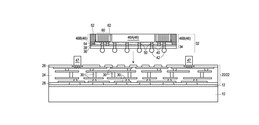
Figure 1: Multi-TIM packages and method Forming Same (US20220359339).
Composite and Graphite TIMs
To improve TIM reliability under aggressive thermal cycling, TSMC combines material hybridization with microstructural control. Composite TIMs embed metal-coated polymer particles within a high-conductivity metal matrix, preserving thermal performance while introducing mechanical compliance that buffers stress, improves thickness uniformity, and reduces die cracking (patent US11107747). In parallel, graphite-based TIMs valued for their exceptional in-plane thermal conductivity but limited by fragility and poor adhesion are stabilized using spacer frames that mechanically isolate the graphite layer, control compression, and prevent interfacial damage (patent applicationUS20250309071). For metal TIMs, where long-term reliability is often degraded by intermetallic compound growth and Kirkendall voiding, TSMC adopts crystallographic engineering: a highly textured Cu (111) diffusion barrier suppresses atomic interdiffusion without sacrificing thermal conductivity (patent application US20250118615), while directly bonded metal TIMs in lid-less or ring-based CoW architectures eliminate remelting risks during reflow (patent application US20250349654). Together, these approaches show that TIM reliability is achieved not by material choice alone, but by precise control of composition, structure, and interfaces.
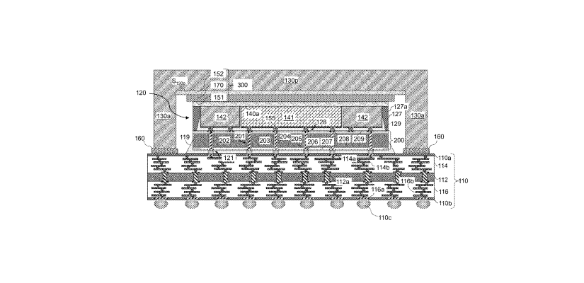
Figure 2: Package structure including a heat dissipation structure and methods of forming the same (US20250118615).
2. Rethinking Heat Paths in 3DIC and Heterogeneous Packages
In 3D stacked-die packages, heat can become trapped because inner dies are partially insulated by underfill and molding compounds, which promotes localized hot spots and thermal crosstalk between layers. To overcome this, TSMC-style architectures shift TIM from a simple “flat” interface into an active 3D thermal network: thermally conductive lids paired with tightly controlled TIM dispensing create more direct heat-flow paths out of stacked dies (patent US11482465); differentiated heat paths, using multiple TIMs and targeted heat-sink protrusions, prioritize high-power dies while avoiding unnecessary metallization for low-power dies (US20240363474); and micro-channels/cavities etched into die and/or lid surfaces, then filled with TIM, expand effective contact area and boost hotspot cooling (CN121096975). The key insight across these patents is that TIM placement and geometry are co-designed with package structure to build vertical, die-specific heat routes rather than relying on a single planar thermal interface.
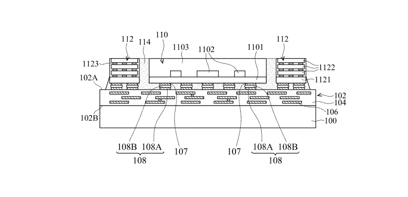
Figure 3: Method for forming semiconductor die package with thermal management features (US20240363474).
TSMC’s approach to thermal management in advanced 3DIC packaging is co-designed thermal and mechanical engineering: heat removal and package deformation (warpage/stress) are treated as coupled problems that directly impact bond quality, interconnect reliability, and yield. Across these patent filings, the recurring failure mode is that higher integration density raises heat flux while stacked-material CTE/property mismatches amplify stress during bonding and thermal cycling, together driving hotspots, warpage, and “non-bond” electrical defects that can escalate into circuit failure.
To address this, the patents describe multiple, complementary hardware/process levers that create better heat paths and better mechanical stability. These include (1) thermally functional gap-fill regions engineered to conduct heat while also absorbing/redistributing stress to reduce warpage (US12249566), (2) a supporting substrate structure over the die that simultaneously serves as a mechanical stiffener and an efficient thermal conduction route—sometimes paired with dummy dies/material selection to balance stress (US20250266318), and (3) top-side heat extraction architectures using a thinned carrier die with aligned dummy pads that pull heat upward through front-side interconnects for more effective dissipation (US20250300149). In parallel, TSMC also claims manufacturing flows (carrier + debonding layer, controlled stacking/release sequences) that make these 3D assemblies more manufacturable and reliable at scale, indirectly supporting thermal solutions by improving alignment/bonding integrity and package robustness (US20250167060).
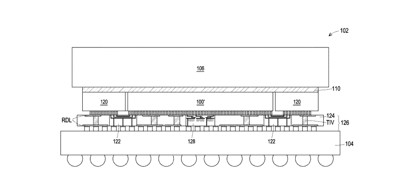
Figure 4: 3DIC with heat dissipation structure and warpage control (US20250266318).
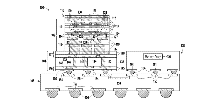
Figure 5: 3DIC packaging with efficient heat dissipation (US20250300149).
Conclusion
In summary, TSMC addresses thermal management in advanced packaging by elevating it to a core design discipline built on two reinforcing pillars: 3DIC architecture innovation and TIM engineering. Rather than treating heat removal, warpage, and reliability as separate issues, TSMC co-designs package structures and thermal interfaces to create efficient heat paths while simultaneously controlling mechanical stress. Architected 3DIC solutions, such as gap-fill thermal structures, supporting substrates, and top-side heat extraction, work in tandem with segmented, composite, and microstructure-engineered TIMs to balance thermal performance, manufacturability, and long-term reliability. This holistic strategy positions thermal management not as a bottleneck, but as a key enabler for scaling power-dense AI, HPC, and heterogeneous systems.
Press contact
contact@knowmade.fr
Le Drakkar, 2405 route des Dolines, 06560 Valbonne Sophia Antipolis, France
www.knowmade.com
About the author
Pauline Calka, PhD. works for KnowMade as a patent analyst in the fields of semiconductor manufacturing and advanced packaging. She holds a PhD in Memory from the University of Grenoble Alpes (France), in partnership with the CEA-Leti (France). After an Alexander von Humboldt Postdoc fellowship position at the Technical University of Berlin (Germany) and the Leibniz Institute for High Performance Microelectronics on ReRAM development, Pauline worked five years at ASM International (Belgium) as Senior Process Engineer on thin film development for logic, memory and MEMS, and two years at CEA-Leti as Integration Engineer on imaging CMOS sensors.
About KnowMade
KnowMade is a technology intelligence and IP strategy firm specializing in the analysis of patents and scientific publications. We assist innovative companies, investors, and research organizations in understanding the competitive landscape, anticipating technological trends, identifying opportunities and risks, improving their R&D, and shaping effective IP strategies.
KnowMade’s analysts combine their strong technology expertise and in-depth knowledge of patents with powerful analytics tools and methodologies to transform patent and scientific data into actionable insights to support decision-making in R&D, innovation, investment, and intellectual property.
KnowMade has solid expertise in Semiconductors and Packaging, Power Electronics, Batteries and Energy Management, RF and Wireless Communications, Photonics, MEMS, Sensing and Imaging, Medical Devices, Biotechnology, Pharmaceuticals, and Agri-Food.