Which companies own patents in microLED display? What are their major thrust areas and portfolio strength?
Publication January 2018
| Download Flyer | Download Sample |
Report’s Key Features

- PDF > 300 slides
- Evolution of patent filings and countries of patent filing
- Key patent analysis, by technology node (chip transfer, chip design, color conversion, defect management, etc.)
- Profiles of filing companies (company type, headquar ters)
- Analysis of key companies’ por tfolios, including portfolio strength index, blocking potential, and IP collaboration networks between players
- Technologies non-specific to microLED displays but impor tant for the field: micro/nano LED, wired LEDs, mass micro-chip transfer
Other related patent landscape reports on photonics, lighting and display-technology. Advance your patent strategy with our custom studies and in-depth patent landscape analysis.
A broad range of actors
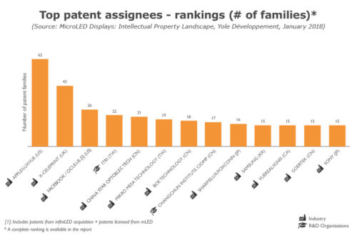 Yole Développement has identified close to 1,500 patents filed by 125 companies and organizations relevant to the microLED display field. Among these are multiple startups, display makers, OEMs, semiconductor companies, LED makers, and research institutions. The overall corpus is relatively young, with an average age of 3.2 years across all families. The first patents were filed in 2000 – 2001, but the bulk of activity started after 2012. Thus, only a minority of patents have been granted so far. Pioneers include Sony, Sharp, MIT, and others, although the bulk of initial developments were conducted by a variety of research institutions including Kansas State University, University of Hong Kong, Strathclyde University & Tyndall Institute (which spun-off mLED, InfiniLED, and X-Celeprint), University of Illinois, and startup companies like Luxvue and, later on, Playnitride and Mikro Mesa. Yole Développement’s study also reveals a number of companies that have not yet been identified as players in the microLED display field. Moreover, our study confirms the commitment of many more companies, i.e. Intel and Goertek, which are not typically associated with display technology. On the flip side, various companies known to be active in the field, i.e. Huawei, have yet to publish any patents in the field. Overall, the field is led mostly by startups and research institutions. With the exception of Sharp and Sony, display makers and LED makers are relative latecomers. Many companies started ramping up their microLED research and development activities after Apple showed faith in microLED with its acquisition of Luxvue. As of December 2017, Apple appears to have the most complete IP portfolio, covering almost all key technology nodes. However, many Apple patents pertain to the technological ecosystem developed around the company’s MEMS transfer technology. Other companies like Sony, with a smaller portfolio but which had a head start, might own more fundamental design patents with strong blocking power.
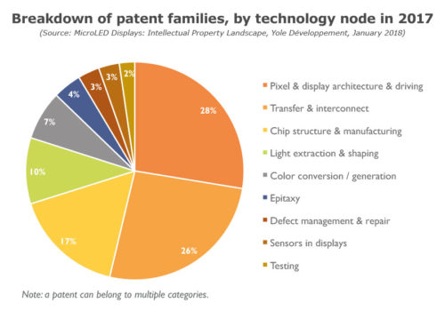
Transfer and display structure dominate, while defect management surprisingly falls behind
Many patents include descriptions of display concepts and architectures. But in terms of manufacturing technologies, pixel transfer & assembly is, not surprisingly, the major topic discussed in invention disclosures. The ability to precisely assemble many millions of small LED chips in a costly, timely fashion, and with very high yields, has long been considered a key enabler for microLED displays. Dozens of possible solutions are presented from more than 50 organizations. Some appear to have given serious thought, and have explored credible development strategies to tackle the challenges. But many other applications only vaguely describe an idea or concept. Despite the diversity of solutions discussed, they can be organized in less than 10 major families, including MEMS, elastomer stamps, fluidic transfers, sticky tapes, etc. Right behind transfer aspects are chip design and manufacturing technologies, since microLEDs currently suffer from much lower efficiency than their traditional “macro” counterparts. New structures and manufacturing processes are required to improve efficiency and make the chips suitable for transfer & assembly, or optimize the emission beam pattern for display applications. More surprising is the relatively few number of applications relating to defect management and microLED testing. These aspects are considered to be key enablers since even with extremely high manufacturing yields defective pixels will remain, and a defect management strategy is required.
A complex supply chain?
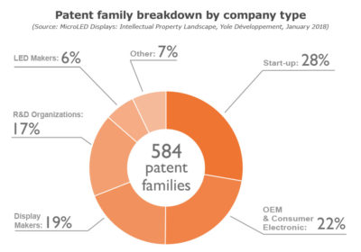 Enabling large-scale microLED display manufacturing requires bringing together three major disparate technologies and supply chain bricks: LED manufacturing, backplane manufacturing, and microchip mass transfer & assembly. The supply chain is complex and lengthy compared to typical displays. Every process is critical and it’s a challenge to effectively manage every aspect. No one company appears positioned to master and execute across a supply chain that will likely be more horizontal, compared to other established display technologies. The IP landscape reflects these challenges through the variety of players involved, but requirements differ from one application to another. For low-volume, high added-value applications like microdisplays for augmented/mixed reality for the enterprise, military, and medical markets, one can envision a well-funded startup with good technology efficiently managing the supply chain. However, consumer applications such as TVs and smartphones will require significant investments to unlock large-scale manufacturing. Though only a few companies have a broad IP portfolio covering all major technology nodes (transfer chip structure, display architecture, etc.), enough players have patents across many technology bricks to guarantee that complex licensing and legal battles will arise once microLED displays enter volume manufacturing and reach the market. Small companies with strong positions in various technology bricks will attempt to obtain licensing fees from larger players involved in manufacturing. Large corporations will try to block each other and prevent their competitors from entering the market. To prepare for such events, some latecomers appear to be filing large quantities of patents, sometimes with little substance.
Companies cited in the report (non exhaustive list)
3M, Aledia, Apple/Luxvue, Atom Nanoelectronics, Au Optronics, Bai Hangkong, Beijing University Of Technology, BOE Technology, CEA, Changchun Institute, CIOMP, CNRS, Columbia University, Cooledge Lighting, Corning, Cree, CSOT, Delta Electronics, Emagin, ETRI, Facebook-Oculus, Focus Lightings Technology, Fraunhofer, Fudan University, Fuzhou University, Glo, Goertek, Google/X Development, Guangdong Poly Optoelectronic, Hahotech, HC Semitek, Epilight, Hiphoton, JD Display, Huawei, III-N Technology, Innolux, Intel, ITRI, Itswell, Jasper Display, Jiangsu Xinguanglian Semiconductor, Junwan Microelectronic Technology, KAIST, Kansas State University, KIMM, Kookmin University, Korea Advanced Nano Fab Center, KOPTI, Lextar Electronics, LG, Lumens, MIT, Mikro Mesa, mLED, Nanjing University Of Technology, Nano & Advanced Materials Institute, Nanometrix, National Taiwan University, Nthdegree, Opto Tech, Osram OS, Ostendo, Penn State Research Foundation, Playnitride, PSI Corp, QMAT, Rohinni, Samsung, Sanan Optoelectronics, Sanken Electric, Seoul Semiconductor, Sharp/Elux/Foxconn, Siliconcore Technology, Sony, Sumitomo Chemical, Sun Yat-Sen University, Sundiode, SUSTC, Sxaymiq Technologies, Tianma, Truly, Tsinghua University, UDC- Universal Display, Unimicron Technology, University Of Hong Kong, University Of Illinois, University Of Pennsylvania, University Of Strathclyde, Versatilis, Vuereal, X-Celeprint, Zena Technologies, Zheng Qingtuan, and more…