More players on the playground, business is starting: when will the IP battle begin?
Publication Apr. 2014
| Download Flyer | Download Sample |
Report’s Key Features

- PDF > 180 slides
- Analysis of technology key segments and key players
- Focus on key technology issues:
- Defect redcution,
- Stress management,
- Buffer type,
- Non-polar GaN,
- GaN on Si(001),
- Layer transfer technology
- Focus on 15 key players including with key patents, patented technologies, partnerships, IP strength and strategy.
- Excel database with all patents of the company profiled in the report
All KnowMade reports on materials and substrates in the semiconductor field. Advance your patent strategy with our custom studies and in-depth patent landscape analysis.
GaN-on-Si is entering production: What is the patent situation?
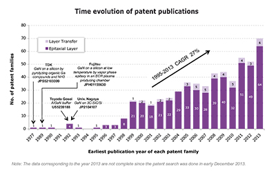
GaN-on-Si technology appeared naturally as an alternative to GaN-on-Sapphire—the main stream technology for LED applications. Today, despite potential cost benefits, the mass adoption of GaN-on-Si technology for LED applications remains unclear. Most major LED makers have a patenting activity related to GaN-on-Si technology, but so far, few have made it the core of their strategy and technology roadmap. Contrary to the LED industry, we expect GaN-on-Si to be widely adopted by Power Electronics and RF applications because of its lower cost and CMOS compatibility. The growth of GaN-on-silicon substrate was first reported in the early-1970s (T. L. Chu et al., J. Electrochemical Society, Vol. 118, page 1200), since the early 1990s more and more academics and industrials have been involved in developing this technology. GaN-on-Si technology is now poised for a list of technical challenges. The high lattice mismatch between GaN and Si results in a high defect density in epitaxial layers (dislocations). The high thermal expansion coefficient (TCE) mismatch between GaN and Si leads to a large tensile stress during cooling from the growth temperature to room temperature. The tensile stress causes film cracking and a concave bending of the wafer (warpage). These factors combine to make both dislocation density and crack/warpage reduction a challenging task. This patent investigation covers patents published worldwide up to December, 2013. The patents addressing the above mentioned challenges have been selected, and an in-depth analysis of patent holders and corresponding patented technologies is provided. This report does not include patents related to active layers or GaN-based devices. Fundamental patents describing a gallium-nitride-based compound semiconductor grown on a silicon substrate were filed before the 1990s with the most significant assigned to TDK and Fujitsu. In the early 1990s, Toyoda Gosei and the University of Nagoya filed the first concepts of a buffer layer for improving the crystallinity of GaN. Those fundamental patents have been followed by an ever increasing number of applications since 1995 as more companies competed in GaN-on-Si technology to meet the technological challenges, the market demand and to lower manufacturing costs. Currently, the patented technologies reflect the significant improvements that have been made on key material issues such as dislocation density reduction and stress management for preventing cracks and warpage of the wafer. According to our analysis, GaN-on-Si IP is mature enough to initiate mass production.
Define your patent strategy with a deep patent segmentation and an useful patent database
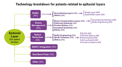
Our search strategy combines automated and manual screenings that have led to the selection of more than 560 relevant patent families. Those have been manually segmented by type (epitaxial layer, layer transfer) and organized in various technology segments that are analyzed in detail: defect reduction (ELOG, pendeoepitaxy, nanomasking, defect selective passivation …), stress management (AlN-based interlayer, buffer engineering, patterned substrate, compliant substrate…), and type of buffer (Al-containing single layer, compositionally graded AlGaN, superlattices…). For each segment, the report provides a detailed analysis including the time evolution of patent filings, identification of the key players and collaboration networks. More than 60 key patents have been identified based on several indicators (family size, legal status, citations analysis, and impact in GaN-on-Si technology…). An excel database with all patents analyzed is also included with the report. This database allows multi-criteria searches and includes; patent publication number, hyperlinks to the original documents, priority date, title, abstract, patent assignees, technological segments, and legal status for each member of the patent family.
Identify key players and discover new IP challengers
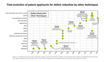
More than 50 companies and academics are involved in GaN-on-Si IP, and most of the major GaN players are present in the list of the top patent applicants. Toyoda Gosei, Toshiba, Panasonic, Mitsubishi, Nitronex, Soitec, and Azzurro have strong IP portfolios related to GaN-based epitaxial layers on Silicon. But Samsung, Dowa, LG, Sharp, and NGK Insulators are becoming major forces in the GaN-on-Si IP landscape. Soitec and Sumitomo lead patent filings related to GaN layer transfer on Si substrate. The report provides a ranking and analysis of the relative strength of the top GaN-on-Si patent holders derived from their portfolio size, patent citations networks, countries of patent filings, and current legal status of patents. Based on this portfolio analysis, we have identified 15 major players that are profiled in this report. Each profile includes: a detailed portfolio summary with patenting activity, patented technologies, key patents, granted patents near expiration, partnerships, and IP strength and strategy.
What is the future for GaN-on-Si IP?
Today, there are only a few players selling either epiwafers or templates – or both – on the open market. The number of commercial GaN-on-Si device makers is also limited. Apart from a few noticeable IP collaborations (Nitronex / International Rectifier, Toshiba / Bridgelux, Soitec / Sumitomo, Macom (Nitronex)/IQE), the GaN-on-Si IP has not yet been widely used by companies as leverage to negotiate licensing and supply agreements. So far, only a few litigations have been observed. However, the existing IP covers all subjects related to the technical challenges, and these last 5 years we have witnessed a reinforcement of critical patent filings by major GaN players (Toshiba, Samsung, LG, Sharp, NGK, Sumitomo, Soitec, Azzurro and Dowa). Furthermore, the GaN-on-Si industry is beginning to take shape as evidenced by the recent interest of the RF/Power industrials for the GaN-on-Si technology (Nitronex acquired by MACOM) and the will of several firms to move onto the production stage (Toshiba, Samsung …). Therefore, the IP battle should be expected in the next 3 years.