
Who has the ability to hamper the development of products using hybrid bonding processes?
Publication November 2019
| Download Flyer | Download Sample |
Report’s Key Features

- PDF with > 80 slides
- Excel file > 1,000 patents
- IP trends, including time-evolution of published patents, countries of patent filings, etc.
- Ranking of main patent assignees
- Key players’ IP position and relative strength of their patent portfolios
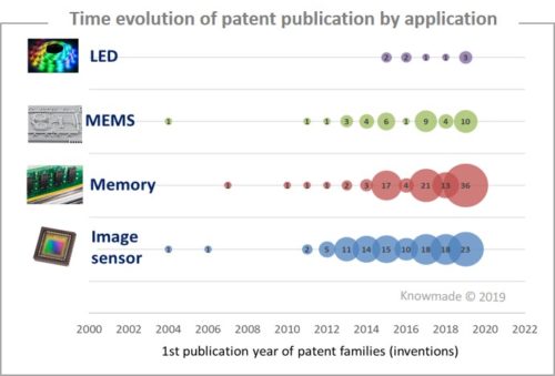
- Patent segmentation per application:
- CMOS image sensor (CIS)
- Memory
- MEMS
- LED
- Key patent identification and details
- IP profile of key players: Xperi, TSMC, YMTC
- Excel database containing all patents analyzed in the report, including technology and application segmentations
KnowMade patent landscapes on advanced packaging for semiconductor technologies. Our patent landscape reports contain the aforementioned useful information that helps decision-makers understand a given innovation or technology.
A technology driven by CIS but on its way to conquer other industries
 The pace of Moore’s law is slowing, if it has not already stopped, as mentioned by Forbes and Nvidia. It’s reaching its limits because developing smaller technology nodes is doable technically, but is no longer cost efficient. The digital electronics market requires a higher density semiconductor memory chip to cater to recently released central processing unit (CPU) components. To answer the growing demand and overcome Moore’s law’s limits, multiple die stacking has been suggested as a solution. Advanced packaging technology development, specifically 2.5D technology, was first used in high performance applications. Today, scaling the Z axis is becoming more and more important in what is called 3D stacking.
Generally, 2.5D-3D stacking was achieved thanks to Through Silicon Via (TSV) technology. However, TSVs are large and using them limits efforts to reach very dense architectures. Furthermore, filling TSVs with metals is complex and requires significant know how. To overcome these limitations, players have started to look at other solutions. A first step toward a new way of 3D stacking is ZiBond, developed by Ziptronix, a company founded in 2000 as a spin-out of Research Triangle Institute. ZiBond is an enhanced version of direct oxide bonding that involves wafer-to-wafer processing at low temperatures, from 150-300°C, to initiate high bond strengths, rivaling silicon. The next step was to combine the dielectric bond with embedded metal to simultaneously bond wafers or bond dies to wafers and form the interconnects. ZiBond is the dielectric bond that forms the basis for direct bonding interconnect (DBI) technology developed in 2005. Tessera, now called Xperi, acquired Ziptronix in 2015 and ZiBond and DBI were integrated in the Invensas subsidiary’s portfolio. This hybrid bonding technology is quickly becoming recognized as the preferred permanent bonding path to form high-density interconnects in heterogeneous integration applications, from 2D enhanced, to 3D stacking with or without TSVs, as well as MEMS.
After entering the CMOS Image Sensor (CIS) market in 2016, hybrid bonding technology has started to be investigated by other industries, such as memory. However, the hybrid bonding market’s growth follows Xperi’s developments. The company has adopted an aggressive strategy to assert its patents. Yet in parallel with the market and Xperi’s growth, some other players, like YMTC, Sony, Samsung and TSMC, have developed their own patent portfolios and strategies and are on the edge of releasing their first products using hybrid bonding processes. Understanding the IP landscape is becoming key to evaluate the risks and opportunities that go with the development and use of hybrid bonding technology.
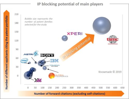
Main IP player ranking
In this report, Knowmade has manually selected more than 290 patent families and inventions related to hybrid bonding and provides a general overview of today’s IP landscape trends and dynamics. Knowmade delivers an understanding and analysis of the current IP positions of the main IP players using or developing hybrid bonding process, as well as the links between them through licensing.
IP player current developments
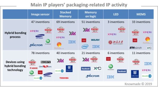
This report reveals all players developing IP related to hybrid bonding per type of targeted applications and shows companies’ current developments. Learn how they integrate hybrid bonding in their manufacturing process flow. Detect your future competitors or partners and evaluate their know how, IP strength, IP weaknesses and the risk of infringing their patents.
Main IP players’ portfolio analysis
This report provides a detailed comparison of the three main IP players’ portfolios: TSMC, Xperi and YMTC. For each player, Knowmade highlights their strengths and weaknesses, and provides information regarding their IP strategies, blocking potential, current and potential licensees. Knowmade also gives an understanding of how these players’ IP could impact the business of companies using or developing hybrid bonding. In addition, a detailed description and analysis of their key patents is provided.
This report’s main assets
• Understanding the key players’ patented technologies and current IP strategies
More than 50 patent applicants are involved in the hybrid bonding patent landscape. This report reveals the IP position of key players through a detailed analysis of their patent portfolios. We also describe their patented technologies, their IP strategy, and their ability to limit other firms’ patenting activity and freedom-to-operate.
• Analyzing IP players’ position, key patents and targeted market
This report furnishes an understanding of IP players’ positions. The main IP players and key patents are presented, along with an understanding of the current applications aimed by players and position in the supply chain.
• Understanding the impact of players IP on the market
This report offers a detailed analysis the blocking potential of each players. Learn about IP players’ capability to limit your freedom to operate and possible ways to by-pass their patents.
• Useful Excel patent database
This report also includes an Excel database with the >1,000 patents and patent applications analyzed in this study. This useful patent database allows for multi-criteria searches and includes patent publication numbers, hyperlinks to the original documents, priority date, title, abstract, patent assignees, patent’s current legal status and application segments.
Companies mentioned in this report (non-exhaustive list)
XPERI, TSMC, YMTC, SAMSUNG ELECTRONICS, SONY, CEA, CANON, RENESAS ELECTRONICS, RAYTHEON, APPLE, STMICROELECTRONICS, SMIC, INTEL, SEOUL NATIONAL UNIVERSITY INDUSTRY FOUNDATION, SHANGHAI IC R&D CENTER, XMC, OMNIVISION TECHNOLOGIES, IMEC, MONOLITHIC 3D, NANYA TECHNOLOGY, KATHOLIEKE UNIVERSITEIT LEUVEN, GLOBALFOUNDRIES, AMERICAN BUSINESS GRID IC TECHNOLOGY, ON SEMICONDUCTOR, QUALCOMM, NCAP, LEXVU OPTO MICROELECTRONICS TECHNOLOGY, INTELLECTUAL VENTURES, MAGNACHIP SEMICONDUCTOR, IBM, ATRI, INSTITUTE OF MICROELECTRONICS CHINESE ACADEMY OF SCIENCES, and more.