SOPHIA ANTIPOLIS, France – May 6, 2019: Nanopore sequencing is one of the next-generation sequencing (NGS) technologies believed to be capable of revolutionizing DNA analysis. Nanopore sequencing is performed using an electrical detection method, which generally includes transporting a sample through the nanopore, which is immersed in a conducting fluid, and applying electric potential across the nanopore. Electric current resulting from the conduction of ions through the nanopore is measured. The magnitude of the electric current density across a nanopore surface depends on the nanopore dimensions and the composition of the sample, such as DNA or RNA, which is occupying the nanopore at the time. Different nucleotides cause characteristic changes in electric current density across nanopore surfaces. These electric current changes are measured and used to sequence the DNA or RNA sample. Different modalities of nanopore sequencing have been developed over time, including protein nanopores, solid-state nanopores, and hybrid nanopores. The technology enables production of ultra-long reads at very high speeds, reducing sample preparation time as well as the data-processing time required to reassemble the reads into their original sequence. Solid-state nanopores are cheaper to produce as they are formed by drilling a nanometer-sized hole in an inorganic substrate. Silicon-derived substrates played an important role in the early development of solid-state nanopores. Indeed, using these substrates allowed to manufacture solid-state nanopores with conventional semiconductor processes (electron/ion beam sculpting, etching). These substrates are also interesting when the electrical detection method is used because they allow to form the electrodes with well-known processes (e.g. serigraphy, lithography). Another interesting feature of solid-state nanopore is its rigid structure preventing the nanopore from moving on the substrate surface.
 Knowmade has shown in its report “Nanopore sequencing patent landscape” published in February 2019 that several companies with strong experience in microelectronics and semiconductors (e.g., Hitachi, IBM, Samsung Electronics, Intel, Qualcomm or GlobalFoundries ) have recently filed patents claiming solid-state nanopores. Moreover, in its patent monitoring services, Knowmade has identify 4 new patent families published in March 2019 in the field of nanopore sequencing filed by Applied Materials (a major supplier in the semiconductor industry). It is very interesting to note that this is the first time that Applied Materials published patents in this field. These patent families include PCT and pending U.S. applications (WO2019/060052, WO2019/060172, WO2019/060042 and WO2019/060168). Inventors of these patents are Philip A. Kraus (Vice President at Applied Materials), Johnson Joseph (Process Engineer at Applied Materials), Mangesh Bangar (Process Engineer – Industrial lithography at Applied Materials), Kenichi Ohno (Process Engineer – semiconductor thin film development at Applied Materials), Zohreh Razavi Hesabi (Process Engineer at Applied Materials) and Ankit Vora (MTS Chemist, now Research Scientist / Chemist at Facebook).
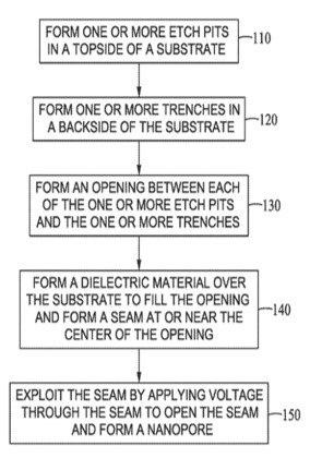
From a technological point of view, these patents filed by Applied Materials claim methods for forming a solid-state nanopore by processes including atomic layer deposition (ALD), and etching; methods to create a free-standing membrane for nanopore sequencing, methods of high scale manufacturing membranes having solid-state nanopores therethrough, and methods for fluidic addressing of the nanopores.
Benefits of these patents include the ability to quickly form well-controlled (size and position) nanopores and nanopore arrays. These methods provide improved signal-to-noise ratios because the size of the nanopore is similar to the size of a single strand of DNA, being transmitted through the nanopore, which increases the change in electric current passing through the nanopore.
These methods also provide free-standing membranes for DNA sequencing applications, that are thin, for example, less than or equal to 1 nm, dielectric, chemically resistant to saline solutions (KCl), have high selectivity to chemistry of etch processes, are physically and electrically pinhole free, have low stress, and are wettable. The thinner the freestanding membrane, the more electrical field will concentrate around the edge of the nanopore, thus, the thinness of the free-standing membranes fabricated according to methods described by Applied Materials allows for high signal-to-noise ratio during the DNA base identification. 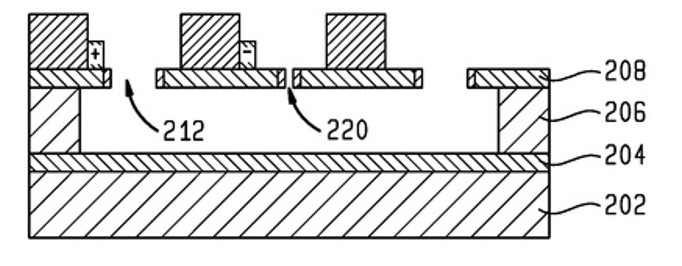
These new patents show that solid-state nanopore sequencing technology attracts more and more players from the semiconductor industry. Indeed, their know-how in the field of semiconductors and nanoscale engineering is very useful for this type of biological application.
More patent landscape analyzes of life sciences technologies by KnowMade.
Press contact
contact@knowmade.fr
Le Drakkar, 2405 route des Dolines, 06560 Valbonne Sophia Antipolis, France
www.knowmade.com
About our analyst
Olivier Thomas, MSc, Olivier works at Knowmade in the field of Biotechnology and Life Sciences. He holds an MSc in Molecular and Cellular Biology from Paris VI University (France). He also holds an Industrial Property International Studies Diploma in Patents and Trademarks from the CEIPI (Strasbourg, France).
About Knowmade
Knowmade is a Technology Intelligence and IP Strategy consulting company specialized in analysis of patents and scientific information. The company helps innovative companies and R&D organizations to understand their competitive landscape, follow technology trends, and find out opportunities and threats in terms of technology and patents.
Knowmade’s analysts combine their strong technology expertise and in-depth knowledge of patents with powerful analytics tools and methodologies to turn patents and scientific information into business-oriented report for decision makers working in R&D, Innovation Strategy, Intellectual Property, and Marketing. Our experts provide prior art search, patent landscape analysis, scientific literature analysis, patent valuation, IP due diligence and freedom-to-operate analysis. In parallel the company proposes litigation/licensing support, technology scouting and IP/technology watch service.
Knowmade has a solid expertise in Compound Semiconductors, Power Electronics, Batteries, RF Technologies & Wireless Communications, Solid-State Lighting & Display, Photonics, Memories, MEMS & Solid-State Sensors/Actuators, Semiconductor Manufacturing, Packaging & Assembly, Medical Devices, Medical Imaging, Microfluidics, Biotechnology, Pharmaceutics, and Agri-Food.