SOPHIA ANTIPOLIS, France – October 1, 2021 | China’s largest LED chip maker, Sanan Optoelectronics, is accelerating its strategy to become a leading silicon carbide (SiC) device supplier, anticipating a take-off in demand from the Chinese automotive market over the next decade. Indeed, the project of a mega-fab in Changsha (Hunan, China) that could handle every step of SiC device fabrication, from crystal growth to device packaging, started just a year ago with the establishment of a subsidiary, Hunan Sanan Semiconductor. Less than a year later, the latter announced the completion of the first phase of the site, resulting in a capacity of 15,000 SiC wafers a month (press release here). This is an important milestone given that Sanan Optoelectronics started its activities in compound semiconductor electronic devices in 2014 through a newly formed subsidiary, Sanan Integrated Circuits (Sanan IC). Furthermore, though the company could leverage the old-established epitaxial growth technologies developed for III-V materials used in LEDs, the same was not true for the growth of large-diameter and high-quality SiC bulk monocrystals, which typically required decades of research and development (R&D) from the most established players in the SiC substrate patent landscape, such as Cree / Wolfspeed or Nippon Steel.
How will Sanan Optoelectronics have the ability to achieve such an industrial and technological feat? “Some clues may be found in its patenting activity, more specifically in the patent applications filed by Sanan IC since 2016 (Figure 1), which launched its 6-inch SiC foundry business in 2018”, says Rémi Comyn, PhD, Technology and Patent Analyst Compound Semiconductors and Electronics at Knowmade. Also, Knowmade analyzed the patenting activity of Sanan Optoelectronics’ subsidiaries Hunan Sanan Semiconductor and Nortel New Materials (Nortel), which were both identified as new entrants in the SiC substrate patent landscape (including bulk SiC and SiC epiwafers). Nortel (not to be mistaken for Norstel AB, acquired by STMicroelectronics in 2019) was established in 2017 and is based in Quanzhou (Fujian, China). The startup company develops SiC crystal growth technology based on the physical vapor transport (PVT) process.
At the time of its acquisition by Hunan Sanan Semiconductor in August 2020, Nortel planned to invest 90M USD in an existing production site which would have the equivalent capacity of 36,000 6-inch SiC wafers a year. Furthermore, as shown in Figure 1 and Figure 2, the Quanzhou-based startup company had already filed more than 80 patent applications related to SiC substrates (including growth methods and devices for bulk SiC) and other SiC wafer processing methods (including for instance tools and consumables for SiC polishing). Among the bulk SiC patents, more than 30 inventions focus on growth devices while 10 inventions relate to SiC finishing. As a result, the acquisition of Nortel provided Sanan Optoelectronics with more than 60 additional patents and more than 20 pending patent applications, grouped into 88 patent families (a patent family represents a single invention filed in multiple countries).
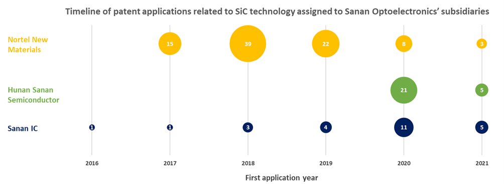
Figure 1: Timeline of all SiC-related patent applications filed by Sanan Optoelectronics’ subsidiaries Nortel, Hunan Sanan Semiconductor and Sanan IC.
What’s more, Hunan Sanan Semiconductor started filing new patent applications from its very foundation in July 2020, which led to 26 domestic patent applications in a single year (Figure 1). Interestingly, Figure 2 indicates that the patenting activity of the newly formed, vertically-integrated company has so far been strongly focused on SiC crystal growth (13 patent families) and other SiC wafer processing tools (13), including for instance a cleaning apparatus, polishing apparatus or apparatus to produce SiC powders. Just like Nortel, Hunan Sanan Semiconductor’s inventions focus on apparatuses for SiC crystal growth and other SiC wafer processing tools (Figure 2).
Interestingly, all of Sanan Optoelectronics’ patents related to SiC epi-wafers were filed by Sanan IC (Figure 2): two patents relate to epitaxial growth equipment, another patent relates to thinning and finishing of a SiC bare wafer or SiC epitaxial wafer, and only one patent relates to epitaxial layers for a SiC-based BJT (Bipolar Junction Transistor) or SiC-based IGBT (Insulated Gate Bipolar Transistor). Sanan IC is also the only assignee among Sanan Optoelectronics’ subsidiaries to file patent applications related to SiC devices: at least 20 patent families have been filed since 2016, with 12 inventions related to SiC diodes and 5 inventions related to SiC MOSFET (Metal Oxide Semiconductor Field Effect Transistors), especially MOSFET with a planar gate structure (planar MOSFET). Some additional patent applications – categorized in Figure 2 as other patents related to SiC device processing – deal with dicing device wafers using laser techniques (2) or forming n-type and p-type ohmic contacts on the same wafer without degradation during subsequent annealing (1).
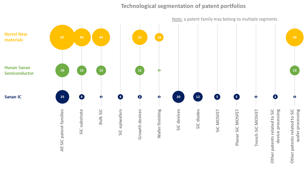
Figure 2: Technological segmentation of the total patent portfolios of Nortel and Hunan Sanan Semiconductor, and technological segmentation of Sanan IC‘s SiC-related patent portfolio.
“Overall, about 60% of Sanan Optoelectronics’ SiC patent portfolio has been granted (84 patents), mainly in China where almost 95% of the patent applications were filed”, notes Rémi Comyn. Indeed, only 8 foreign applications have been filed since 2016 by Nortel (4 PCT applications), Sanan IC (2 PCT applications, 1 US application) and Hunan Sanan Semiconductor (1 US application). Nortel’s international applications deal for example with multi-line cutting methods, a growth device addressing the non-stoichiometric decomposition when sublimating the SiC powders in a PVT growth reactor, and a growth device without bonding seeds (Figure 3a). Hunan Sanan Semiconductor’s US application relates to an etching tool used to characterize defects in multiple SiC wafers simultaneously. Finally, Sanan IC’s only alive PCT application describes a SiC trench Schottky diode structure (Figure 3b).
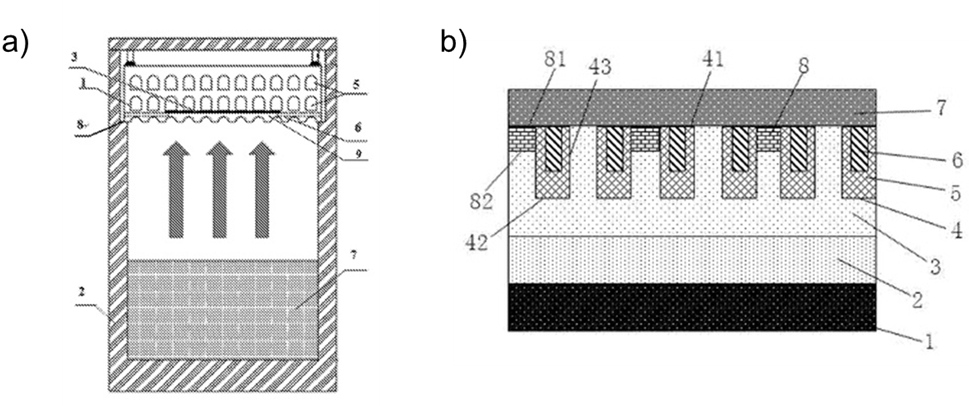
Figure 3: a) PCT application (WO2020/088233) filed by Nortel in 2018: A SiC single-crystal growth device able to reduce the risk of physical injury and crystal damage caused by improper operation during crystal removal. b) PCT application (WO2020/151475) filed by Sanan IC in 2019: A SiC trench Schottky diode device having an anti-surge current capability.
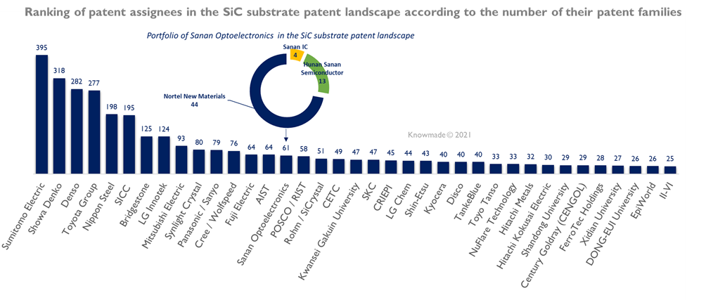
Figure 4: Main patent assignees in the SiC substrate patent landscape.To sum up, the rapid growth of Sanan Optoelectronics’ SiC patent portfolio in less than 5 years – through its subsidiaries Sanan IC and Hunan Sanan Semiconductor – reflects the significant investment in R&D (adding up to a $2.5 billion investment in Changsha mega-fab) made by the leading LED chip maker in SiC semiconductor technology, especially SiC crystal growth technology. “Furthermore, by acquiring a local startup company, Nortel, it strongly consolidated its intellectual property (IP) position in this field, especially regarding the growth device technology for bulk SiC”, points out Rémi Comyn. As a result, despite being a new entrant in the SiC substrate patent landscape (including bulk SiC and SiC epiwafers), Sanan Optoelectronics is already among the top 20 leading patent applicants in terms of number of patent families (Figure 4). “What’s more, its patent portfolio is mostly made up of patents enforceable in China. As such, it represents a serious threat in terms of freedom-to-operate (FTO) to whoever aims to expand its SiC business in China, including SICC, TankeBlue, or Synlight Crystal; but also several foreign players such as Showa Denko or Sumitomo Electric, both leading patent applicants in China for SiC substrates and SiC epiwafers”, adds Rémi Comyn. However, Sanan Optoelectronics has so far been a domestic IP player, and although it exhibits international ambitions as a SiC power device supplier, it is strongly exposed outside China in terms of intellectual property. Still, several foreign patent publications could be granted to Sanan Optoelectronics in the near future, thus providing the company with a better IP position to address the US and European markets in particular.
KnowMade produces in-depth analyzes of patent situation in MEMS, sensing and imaging technologies. Take advantage of our reports.
Press contact
contact@knowmade.fr
Le Drakkar, 2405 route des Dolines, 06560 Valbonne Sophia Antipolis, France
www.knowmade.com
About our analysts
Rémi Comyn, PhD, Rémi works for Knowmade in the field of Compound Semiconductors and Electronics. He holds a PhD in Physics from the University of Nice Sophia-Antipolis (France) in partnership with CRHEA-CNRS (Sophia-Antipolis, France) and the University of Sherbrooke (Québec, Canada). Rémi previously worked in compound semiconductors research laboratory as Research Engineer.
About Knowmade
Knowmade is a Technology Intelligence and IP Strategy consulting company specialized in analysis of patents and scientific information. The company helps innovative companies and R&D organizations to understand their competitive landscape, follow technology trends, and find out opportunities and threats in terms of technology and patents.
Knowmade’s analysts combine their strong technology expertise and in-depth knowledge of patents with powerful analytics tools and methodologies to turn patents and scientific information into business-oriented report for decision makers working in R&D, Innovation Strategy, Intellectual Property, and Marketing. Our experts provide prior art search, patent landscape analysis, scientific literature analysis, patent valuation, IP due diligence and freedom-to-operate analysis. In parallel the company proposes litigation/licensing support, technology scouting and IP/technology watch service.
Knowmade has a solid expertise in Compound Semiconductors, Power Electronics, Batteries, RF Technologies & Wireless Communications, Solid-State Lighting & Display, Photonics, Memories, MEMS & Solid-State Sensors/Actuators, Semiconductor Manufacturing, Packaging & Assembly, Medical Devices, Medical Imaging, Microfluidics, Biotechnology, Pharmaceutics, and Agri-Food.