New nanowire LED startups compete with Asian LED giants in the IP landscape
Publication May. 2014
| Download Flyer | Download Sample |
Report’s Key Features

- PDF > 130 slides
- Analysis of technology key segments and key players
- Focus on key technology issues:
- Deposition method
- Substrate type
- Active material type
- PN junction type
- Passive material type
- Focus on 6 key players including patents, patented technologies, partnerships, and patents nearing expiration
- Excel database with all patents of the company profiled in the report
Connected patent landscapes on the same technology.
A patent landscape analysis contains a wealth of useful information for business owners and policymakers.
Nanowire LED: after 10 years of patenting activity, what’s the current patent situation?
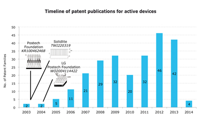
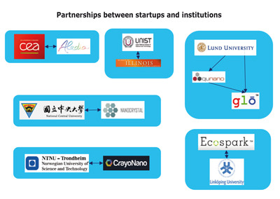
Asian giants Samsung, Panasonic and LG are the top three patent assignees for Nanowire LED technology. Facing them are several startups including glō, Aledia and Ecospark, which between them have raised more than $150M – thus confirming their serious interest in this field. However, these newcomers face strong technological challenges. Nanowire-based LEDs were first reported in the early 2000s by Harvard University (J. American Chemical Soc., 122, 1, 188-189) and National Taiwan Normal University (Adv. Mat., 12, 10, 738). The first patent was filed in 2002 by Postech Foundation for an axial PN junction architecture. Since then, companies have shown growing interest in nanowire-based LED for improved light extraction and thermal conduction. Fundamental patents describing a nanowire-based axial LED were filed during the 2000s, with the most significant ones coming from Postech Foundation, Solidlite and LG. In the mid-2000s, Philips, Nanosys, LG and Seoul Opto Devices filed the first radial/core-shell nanowire LED patents. Current patented technologies reflect the improvements made in terms of material and junction architecture to achieve limited crystal defects and increased luminous efficiency. KnowMade’s research covers global patents published through February 2014. Patents addressing the use of nanowires in LED applications have been selected, and an analysis of the patent holders and their patented technologies is provided. This report focuses exclusively on LED and does not include patents related to the fabrication of nanowires for other applications such as solar, detectors, or laser.
Identify key players and discover new ip entrants
More than 100 companies/academics are involved in Nanowire LED IP, and most of the major Nanowire LED players are slightly different from the major LED players. Samsung, LG and Panasonic have strong IP portfolios related to Nanowire LED, but glō, Ecospark, Hon Hai Precision Industry, Nanocrystal, Lextar Electronics and others are strong new entrants to the Nanowire LED IP landscape. Taking into account their portfolio size, patent citations networks, countries of patents filings and current legal status of patents, this report provides a ranking and relative strength of the top Nanowire LED patent holders. Through thorough analysis we have identified six major players, each of which is profiled in this report. Each profile includes a detailed portfolio summary including patenting activity, patented technologies, key patents, granted patents near expiration, and partnerships.
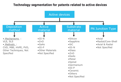
Refine your patent strategy with a deep patent segmentation and a useful patent database
Through a search strategy consisting of automated and manual screenings, we have been able to identify 300+ patent families. For this report, these families are manually segmented by relevance: patents describing LED applications (relevant patents), and patents describing not only LED applications but also other applications (solar, laser, detector etc.) or devices that use LED nanowires (related patents). These 300+ patent families are also manually segmented by technology type: “Active Devices”, i.e. when the PN junction is comprised on the nanowire; and “Passive Devices”, i.e. when the nanowire is out of the PN junction (light extraction enhancement). 246 and 116 patent families are related to active and passive devices, respectively. The dataset is also organized into various technology segments that are analyzed: deposition method, substrate type, active material, passive material and PN junction architecture. III-N and ZnO represent the biggest part of patents related to active and passive devices, respectively. Most patent applicants have filed axial PN junction architecture, but recently they have started turning toward radial PN junction. More than 30 key patents have been identified based on several indicators, including family size, legal status, citations analysis and impact on Nanowire LED technology. Our report also includes an Excel database containing all of the analyzed patents. This database allows for multi-criteria searches and includes patent publication number, hyperlinks to the original documents, priority date, title, abstract, patent assignees, technological segments and legal status for each member of the patent family.